C8051F005DK Silicon Laboratories Inc, C8051F005DK Datasheet - Page 103
C8051F005DK
Manufacturer Part Number
C8051F005DK
Description
DEV KIT FOR F005/006/007
Manufacturer
Silicon Laboratories Inc
Type
MCUr
Datasheet
1.C8051F005-TB.pdf
(171 pages)
Specifications of C8051F005DK
Contents
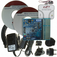
Evaluation Board, Power Supply, USB Cables, Adapter and Documentation
Processor To Be Evaluated
C8051F01x
Interface Type
USB
Silicon Manufacturer
Silicon Labs
Core Architecture
8051
Silicon Core Number
C8051F005
Silicon Family Name
C8051F00x
Lead Free Status / RoHS Status
Contains lead / RoHS non-compliant
For Use With/related Products
Silicon Laboratories C8051 F005/006/007
Lead Free Status / Rohs Status
Lead free / RoHS Compliant
Other names
336-1188
Available stocks
Company
Part Number
Manufacturer
Quantity
Price
Company:

Part Number:
C8051F005DK
Manufacturer:
SiliconL
Quantity:
1


15. PORT INPUT/OUTPUT
The MCUs have a wide array of digital resources, which are available through four digital I/O ports, P0, P1, P2 and
P3. Each of the pins on Ports 0, 1, and 2 can be defined as either its corresponding port I/O or one of the internal
digital resources assigned as shown in Figure 15.1. The designer has complete control over which functions are
assigned, limited only by the number of physical I/O pins available on the selected package (the
C8051F000/05/10/15 have all four ports pinned out, the F001/06/11/16 have P0 and P1, and the F002/07/12/17
have P0). This resource assignment flexibility is achieved through the use of a Priority CrossBar Decoder. (Note
that the state of a Port I/O pin can always be read in the corresponding Port latch regardless of the Crossbar
settings).
The CrossBar assigns the selected internal digital resources to the I/O pins based on the Priority Decode Table 15.1.
The registers XBR0, XBR1, and XBR2, defined in Figure 15.3, Figure 15.4, and Figure 15.5 are used to select an
internal digital function or let an I/O pin default to being a Port I/O. The crossbar functions identically for each
MCU, with the caveat that P2 is not pinned out on the F001/06/11/16, and both P1 and P2 are not pinned out on the
F002/07/12/17. Digital resources assigned to port pins that are not pinned out cannot be accessed.
All Port I/Os are 5V tolerant (Refer to Figure 15.2 for the port cell circuit.) The Port I/O cells are configured as
either push-pull or open-drain in the Port Configuration Registers (PRT0CF, PRT1CF, PRT2CF, PRT3CF).
Complete Electrical Specifications for Port I/O are given in Table 15.2.
15.1.
One of the design goals of this MCU family was to make the entire palette of digital resources available to the
designer even on reduced pin count packages. The Priority CrossBar Decoder provides an elegant solution to the
problem of connecting the internal digital resources to the physical I/O pins.
The Priority CrossBar Decode (Table 15.1) assigns a priority to each I/O function, starting at the top with the
SMBus. As the table illustrates, when selected, its two signals will be assigned to Pin 0 and 1 of I/O Port 0. The
decoder always fills I/O bits from LSB to MSB starting with Port 0, then Port 1, finishing if necessary with Port 2.
If you choose not to use a resource, the next function down on the table will fill the priority slot. In this way it is
possible to choose only the functions required by the design, making full use of the available I/O pins. Also, any
extra Port I/O are grouped together for more convenient use in application code.
Registers XBR0, XBR1 and XBR2 are used to assign the digital I/O resources to the physical I/O Port pins. It is
important to understand that when the SMBus, SPI Bus, or UART is selected, the crossbar assigns all pins
associated with the selected bus. It would be impossible for instance to assign the RX pin from the UART function
without also assigning the TX function. Standard Port I/Os appear contiguously after the prioritized functions have
been assigned. For example, if you choose functions that take the first 14 Port I/O (P0.[7:0], P1.[5:0]), you would
have 18 Port I/O left unused by the crossbar (P1.[7:6], P2 and P3).
15.2.
Port I/O initialization is straightforward. Registers XBR0, XBR1 and XBR2 must be loaded with the appropriate
values to select the digital I/O functions required by the design. Setting the XBARE bit in XBR2 to 1 enables the
CrossBar. Until the Crossbar is enabled, the external pins remain as standard Ports in input mode regardless
of the XBRn Register settings. For given XBRn Register settings, one can determine the I/O pin-out using the
Priority Decode Table; as an alternative, the Code Configuration Wizard function of the IDE software will
determine the Port I/O pin-assignments based on the XBRn Register settings.
The output driver characteristics of the I/O pins are defined using the Port Configuration Registers PRT0CF,
PRT1CF, PRT2CF and PRT3CF (see Figure 15.7, Figure 15.9, Figure 15.12, and Figure 15.14). Each Port Output
driver can be configured as either Open Drain or Push-Pull. This is required even for the digital resources selected
in the XBRn registers and is not automatic. The only exception to this is the SMBus (SDA, SCL) and UART
Receive (RX, when in mode 0) pins which are Open-drain regardless of the PRTnCF settings.
WEAKPUD bit in XBR2 is 0, a weak pullup is enabled for all Port I/O configured as open-drain. WEAKPUD does
103
C8051F000/1/2/5/6/7
C8051F010/1/2/5/6/7
Priority Cross Bar Decoder
Port I/O Initialization
Rev. 1.7
When the
Related parts for C8051F005DK
Image
Part Number
Description
Manufacturer
Datasheet
Request
R

Part Number:
Description:
SMD/C°/SINGLE-ENDED OUTPUT SILICON OSCILLATOR
Manufacturer:
Silicon Laboratories Inc
Part Number:
Description:
Manufacturer:
Silicon Laboratories Inc
Datasheet:
Part Number:
Description:
N/A N/A/SI4010 AES KEYFOB DEMO WITH LCD RX
Manufacturer:
Silicon Laboratories Inc
Datasheet:
Part Number:
Description:
N/A N/A/SI4010 SIMPLIFIED KEY FOB DEMO WITH LED RX
Manufacturer:
Silicon Laboratories Inc
Datasheet:
Part Number:
Description:
N/A/-40 TO 85 OC/EZLINK MODULE; F930/4432 HIGH BAND (REV E/B1)
Manufacturer:
Silicon Laboratories Inc
Part Number:
Description:
EZLink Module; F930/4432 Low Band (rev e/B1)
Manufacturer:
Silicon Laboratories Inc
Part Number:
Description:
I°/4460 10 DBM RADIO TEST CARD 434 MHZ
Manufacturer:
Silicon Laboratories Inc
Part Number:
Description:
I°/4461 14 DBM RADIO TEST CARD 868 MHZ
Manufacturer:
Silicon Laboratories Inc
Part Number:
Description:
I°/4463 20 DBM RFSWITCH RADIO TEST CARD 460 MHZ
Manufacturer:
Silicon Laboratories Inc
Part Number:
Description:
I°/4463 20 DBM RADIO TEST CARD 868 MHZ
Manufacturer:
Silicon Laboratories Inc
Part Number:
Description:
I°/4463 27 DBM RADIO TEST CARD 868 MHZ
Manufacturer:
Silicon Laboratories Inc
Part Number:
Description:
I°/4463 SKYWORKS 30 DBM RADIO TEST CARD 915 MHZ
Manufacturer:
Silicon Laboratories Inc
Part Number:
Description:
N/A N/A/-40 TO 85 OC/4463 RFMD 30 DBM RADIO TEST CARD 915 MHZ
Manufacturer:
Silicon Laboratories Inc
Part Number:
Description:
I°/4463 20 DBM RADIO TEST CARD 169 MHZ
Manufacturer:
Silicon Laboratories Inc