C8051F005DK Silicon Laboratories Inc, C8051F005DK Datasheet - Page 125
C8051F005DK
Manufacturer Part Number
C8051F005DK
Description
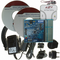
DEV KIT FOR F005/006/007
Manufacturer
Silicon Laboratories Inc
Type
MCUr
Datasheet
1.C8051F005-TB.pdf
(171 pages)
Specifications of C8051F005DK
Contents
Evaluation Board, Power Supply, USB Cables, Adapter and Documentation
Processor To Be Evaluated
C8051F01x
Interface Type
USB
Silicon Manufacturer
Silicon Labs
Core Architecture
8051
Silicon Core Number
C8051F005
Silicon Family Name
C8051F00x
Lead Free Status / RoHS Status
Contains lead / RoHS non-compliant
For Use With/related Products
Silicon Laboratories C8051 F005/006/007
Lead Free Status / Rohs Status
Lead free / RoHS Compliant
Other names
336-1188
Available stocks
Company
Part Number
Manufacturer
Quantity
Price
Company:

Part Number:
C8051F005DK
Manufacturer:
SiliconL
Quantity:
1


17.2.
Only a SPI master device can initiate a data transfer. The SPI is placed in master mode by setting the Master Enable
flag (MSTEN, SPI0CN.1). Writing a byte of data to the SPI data register (SPI0DAT) when in Master Mode starts a
data transfer. The SPI master immediately shifts out the data serially on the MOSI line while providing the serial
clock on SCK. The SPIF (SPI0CN.7) flag is set to logic 1 at the end of the transfer. If interrupts are enabled, an
interrupt request is generated when the SPIF flag is set. The SPI master can be configured to shift in/out from one
to eight bits in a transfer operation in order to accommodate slave devices with different word lengths. The SPIFRS
bits in the SPI Configuration Register (SPI0CFG.[2:0]) are used to select the number of bits to shift in/out in a
transfer operation.
While the SPI master transfers data to a slave on the MOSI line, the addressed SPI slave device simultaneously
transfers the contents of its shift register to the SPI master on the MISO line in a full-duplex operation. The data
byte received from the slave replaces the data in the master’s data register. Therefore, the SPIF flag serves as both a
transmit-complete and receive-data-ready flag. The data transfer in both directions is synchronized with the serial
clock generated by the master. Figure 17.3 illustrates the full-duplex operation of an SPI master and an addressed
slave.
The SPI data register is double buffered on reads, but not on a write. If a write to SPI0DAT is attempted during a
data transfer, the WCOL flag (SPI0CN.6) will be set to logic 1 and the write is ignored. The current data transfer
will continue uninterrupted. A read of the SPI data register by the system controller actually reads the receive
buffer. If the receive buffer still holds unread data from a previous transfer when the last bit of the current transfer
is shifted into the SPI shift register, a receive overrun occurs and the RXOVRN flag (SPI0CN.4) is set to logic 1.
The new data is not transferred to the receive buffer, allowing the previously received data byte to be read. The data
byte causing the overrun is lost.
When the SPI is enabled and not configured as a master, it will operate as an SPI slave. Another SPI device acting
as a master will initiate a transfer by driving the NSS signal low. The master then shifts data out of the shift register
on the MOSI pin using the its serial clock. The SPIF flag is set to logic 1 at the end of a data transfer (when the
NSS signal goes high). The slave can load its shift register for the next data transfer by writing to the SPI data
register. The slave must make the write to the data register at least one SPI serial clock cycle before the master
starts the next transmission. Otherwise, the byte of data already in the slave’s shift register will be transferred.
Multiple masters may reside on the same bus. A Mode Fault flag (MODF, SPI0CN.5) is set to logic 1 when the SPI
is configured as a master (MSTEN = 1) and its slave select signal NSS is pulled low. When the Mode Fault flag is
set, the MSTEN and SPIEN bits of the SPI control register are cleared by hardware, thereby placing the SPI module
125
C8051F000/1/2/5/6/7
C8051F010/1/2/5/6/7
Operation
7
SPI SHIFT REGISTER
Receive Buffer
6
Baud Rate
Generator
5
MASTER DEVICE
4
3
Figure 17.3. Full Duplex Operation
2
1
0
MOSI
MISO
NSS
SCK
Px.y
Rev. 1.7
VDD
MOSI
MISO
NSS
SCK
SLAVE DEVICE
7
SPI SHIFT REGISTER
Receive Buffer
6
5
4
3
2
1
0
Related parts for C8051F005DK
Image
Part Number
Description
Manufacturer
Datasheet
Request
R

Part Number:
Description:
SMD/C°/SINGLE-ENDED OUTPUT SILICON OSCILLATOR
Manufacturer:
Silicon Laboratories Inc
Part Number:
Description:
Manufacturer:
Silicon Laboratories Inc
Datasheet:
Part Number:
Description:
N/A N/A/SI4010 AES KEYFOB DEMO WITH LCD RX
Manufacturer:
Silicon Laboratories Inc
Datasheet:
Part Number:
Description:
N/A N/A/SI4010 SIMPLIFIED KEY FOB DEMO WITH LED RX
Manufacturer:
Silicon Laboratories Inc
Datasheet:
Part Number:
Description:
N/A/-40 TO 85 OC/EZLINK MODULE; F930/4432 HIGH BAND (REV E/B1)
Manufacturer:
Silicon Laboratories Inc
Part Number:
Description:
EZLink Module; F930/4432 Low Band (rev e/B1)
Manufacturer:
Silicon Laboratories Inc
Part Number:
Description:
I°/4460 10 DBM RADIO TEST CARD 434 MHZ
Manufacturer:
Silicon Laboratories Inc
Part Number:
Description:
I°/4461 14 DBM RADIO TEST CARD 868 MHZ
Manufacturer:
Silicon Laboratories Inc
Part Number:
Description:
I°/4463 20 DBM RFSWITCH RADIO TEST CARD 460 MHZ
Manufacturer:
Silicon Laboratories Inc
Part Number:
Description:
I°/4463 20 DBM RADIO TEST CARD 868 MHZ
Manufacturer:
Silicon Laboratories Inc
Part Number:
Description:
I°/4463 27 DBM RADIO TEST CARD 868 MHZ
Manufacturer:
Silicon Laboratories Inc
Part Number:
Description:
I°/4463 SKYWORKS 30 DBM RADIO TEST CARD 915 MHZ
Manufacturer:
Silicon Laboratories Inc
Part Number:
Description:
N/A N/A/-40 TO 85 OC/4463 RFMD 30 DBM RADIO TEST CARD 915 MHZ
Manufacturer:
Silicon Laboratories Inc
Part Number:
Description:
I°/4463 20 DBM RADIO TEST CARD 169 MHZ
Manufacturer:
Silicon Laboratories Inc