C8051F005DK Silicon Laboratories Inc, C8051F005DK Datasheet - Page 20
C8051F005DK
Manufacturer Part Number
C8051F005DK
Description
DEV KIT FOR F005/006/007
Manufacturer
Silicon Laboratories Inc
Type
MCUr
Datasheet
1.C8051F005-TB.pdf
(171 pages)
Specifications of C8051F005DK
Contents
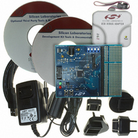
Evaluation Board, Power Supply, USB Cables, Adapter and Documentation
Processor To Be Evaluated
C8051F01x
Interface Type
USB
Silicon Manufacturer
Silicon Labs
Core Architecture
8051
Silicon Core Number
C8051F005
Silicon Family Name
C8051F00x
Lead Free Status / RoHS Status
Contains lead / RoHS non-compliant
For Use With/related Products
Silicon Laboratories C8051 F005/006/007
Lead Free Status / Rohs Status
Lead free / RoHS Compliant
Other names
336-1188
Available stocks
Company
Part Number
Manufacturer
Quantity
Price
Company:

Part Number:
C8051F005DK
Manufacturer:
SiliconL
Quantity:
1


2. ABSOLUTE MAXIMUM RATINGS*
Ambient temperature under bias................................................................................................................. -55 to 125C
Storage Temperature .................................................................................................................................. -65 to 150C
Voltage on any Pin (except VDD and Port I/O) with respect to DGND ................................... -0.3V to (VDD + 0.3V)
Voltage on any Port I/O Pin or /RST with respect to DGND....................................................................-0.3V to 5.8V
Voltage on VDD with respect to DGND...................................................................................................-0.3V to 4.2V
Maximum Total current through VDD, AV+, DGND and AGND .....................................................................800mA
Maximum output current sunk by any Port pin ...................................................................................................100mA
Maximum output current sunk by any other I/O pin .............................................................................................25mA
Maximum output current sourced by any Port pin ..............................................................................................100mA
Maximum output current sourced by any other I/O pin ........................................................................................25mA
*Note: Stresses above those listed under “Absolute Maximum Ratings” may cause permanent damage to the device.
This is a stress rating only and functional operation of the devices at those or any other conditions above those
indicated in the operation listings of this specification is not implied. Exposure to maximum rating conditions for
extended periods may affect device reliability.
3. GLOBAL DC ELECTRICAL CHARACTERISTICS
-40C to +85C unless otherwise specified.
Analog Supply Voltage
Analog Supply Current
Analog Supply Current with
analog sub-systems inactive
Analog-to-Digital Supply
Delta ( | VDD – AV+ | )
Digital Supply Voltage
Digital Supply Current with
CPU active
Digital Supply Current
(shutdown)
Digital Supply RAM Data
Retention Voltage
Specified Operating
Temperature Range
SYSCLK (System Clock
Frequency)
SYSCLK (System Clock
Frequency)
Tsysl (SYSCLK Low Time)
Tsysh (SYSCLK High Time)
Note 1: Analog Supply AV+ must be greater than 1V for VDD monitor to operate.
Note 2: SYSCLK must be at least 32 kHz to enable debugging.
PARAMETER
(Note 1)
Internal REF, ADC, DAC, Comparators
all active
Internal REF, ADC, DAC, Comparators
all disabled, oscillator disabled
VDD = 2.7V, Clock=25MHz
VDD = 2.7V, Clock=1MHz
VDD = 2.7V, Clock=32kHz
Oscillator not running
C8051F005/6/7, C8051F015/6/7
(Note 2)
C8051F000/1/2, C8051F010/1/2
(Note 2)
CONDITIONS
Rev. 1.7
C8051F000/1/2/5/6/7
C8051F010/1/2/5/6/7
MIN
-40
2.7
2.7
18
18
0
0
TYP
12.5
3.0
3.0
0.5
1.5
10
1
5
5
MAX
+85
3.6
0.5
3.6
20
25
20
2
UNITS
MHz
MHz
mA
mA
mA
A
A
A
C
ns
ns
V
V
V
V
20
Related parts for C8051F005DK
Image
Part Number
Description
Manufacturer
Datasheet
Request
R

Part Number:
Description:
SMD/C°/SINGLE-ENDED OUTPUT SILICON OSCILLATOR
Manufacturer:
Silicon Laboratories Inc
Part Number:
Description:
Manufacturer:
Silicon Laboratories Inc
Datasheet:
Part Number:
Description:
N/A N/A/SI4010 AES KEYFOB DEMO WITH LCD RX
Manufacturer:
Silicon Laboratories Inc
Datasheet:
Part Number:
Description:
N/A N/A/SI4010 SIMPLIFIED KEY FOB DEMO WITH LED RX
Manufacturer:
Silicon Laboratories Inc
Datasheet:
Part Number:
Description:
N/A/-40 TO 85 OC/EZLINK MODULE; F930/4432 HIGH BAND (REV E/B1)
Manufacturer:
Silicon Laboratories Inc
Part Number:
Description:
EZLink Module; F930/4432 Low Band (rev e/B1)
Manufacturer:
Silicon Laboratories Inc
Part Number:
Description:
I°/4460 10 DBM RADIO TEST CARD 434 MHZ
Manufacturer:
Silicon Laboratories Inc
Part Number:
Description:
I°/4461 14 DBM RADIO TEST CARD 868 MHZ
Manufacturer:
Silicon Laboratories Inc
Part Number:
Description:
I°/4463 20 DBM RFSWITCH RADIO TEST CARD 460 MHZ
Manufacturer:
Silicon Laboratories Inc
Part Number:
Description:
I°/4463 20 DBM RADIO TEST CARD 868 MHZ
Manufacturer:
Silicon Laboratories Inc
Part Number:
Description:
I°/4463 27 DBM RADIO TEST CARD 868 MHZ
Manufacturer:
Silicon Laboratories Inc
Part Number:
Description:
I°/4463 SKYWORKS 30 DBM RADIO TEST CARD 915 MHZ
Manufacturer:
Silicon Laboratories Inc
Part Number:
Description:
N/A N/A/-40 TO 85 OC/4463 RFMD 30 DBM RADIO TEST CARD 915 MHZ
Manufacturer:
Silicon Laboratories Inc
Part Number:
Description:
I°/4463 20 DBM RADIO TEST CARD 169 MHZ
Manufacturer:
Silicon Laboratories Inc