C8051F005DK Silicon Laboratories Inc, C8051F005DK Datasheet - Page 3
C8051F005DK
Manufacturer Part Number
C8051F005DK
Description
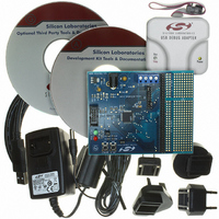
DEV KIT FOR F005/006/007
Manufacturer
Silicon Laboratories Inc
Type
MCUr
Datasheet
1.C8051F005-TB.pdf
(171 pages)
Specifications of C8051F005DK
Contents
Evaluation Board, Power Supply, USB Cables, Adapter and Documentation
Processor To Be Evaluated
C8051F01x
Interface Type
USB
Silicon Manufacturer
Silicon Labs
Core Architecture
8051
Silicon Core Number
C8051F005
Silicon Family Name
C8051F00x
Lead Free Status / RoHS Status
Contains lead / RoHS non-compliant
For Use With/related Products
Silicon Laboratories C8051 F005/006/007
Lead Free Status / Rohs Status
Lead free / RoHS Compliant
Other names
336-1188
Available stocks
Company
Part Number
Manufacturer
Quantity
Price
Company:

Part Number:
C8051F005DK
Manufacturer:
SiliconL
Quantity:
1


6.
7.
8.
9.
10. CIP-51 CPU.......................................................................................................................... 62
3
C8051F000/1/2/5/6/7
C8051F010/1/2/5/6/7
Table 5.1. 12-Bit ADC Electrical Characteristics..............................................................................................38
Table 5.1. 12-Bit ADC Electrical Characteristics..............................................................................................39
ADC (10-Bit, C8051F010/1/2/5/6/7 Only).......................................................................... 40
Figure 6.1. 10-Bit ADC Functional Block Diagram..........................................................................................40
6.1.
6.2.
Figure 6.2. 10-Bit ADC Track and Conversion Example Timing.....................................................................41
Figure 6.3. Temperature Sensor Transfer Function...........................................................................................42
Figure 6.4. AMX0CF: AMUX Configuration Register (C8051F01x) ..............................................................42
Figure 6.5. AMX0SL: AMUX Channel Select Register (C8051F01x).............................................................43
Figure 6.6. ADC0CF: ADC Configuration Register (C8051F01x)...................................................................44
Figure 6.7. ADC0CN: ADC Control Register (C8051F01x) ............................................................................45
Figure 6.8. ADC0H: ADC Data Word MSB Register (C8051F01x) ...............................................................46
Figure 6.9. ADC0L: ADC Data Word LSB Register (C8051F01x).................................................................46
6.3.
Figure 6.10. ADC0GTH: ADC Greater-Than Data High Byte Register (C8051F01x) ....................................47
Figure 6.11. ADC0GTL: ADC Greater-Than Data Low Byte Register (C8051F01x) .....................................47
Figure 6.12. ADC0LTH: ADC Less-Than Data High Byte Register (C8051F01x) .........................................47
Figure 6.13. ADC0LTL: ADC Less-Than Data Low Byte Register (C8051F01x)...........................................47
Figure 6.14. 10-Bit ADC Window Interrupt Examples, Right Justified Data...................................................48
Figure 6.15. 10-Bit ADC Window Interrupt Examples, Left Justified Data .....................................................48
Figure 6.15. 10-Bit ADC Window Interrupt Examples, Left Justified Data .....................................................49
Table 6.1. 10-Bit ADC Electrical Characteristics..............................................................................................49
Table 6.1. 10-Bit ADC Electrical Characteristics..............................................................................................50
DACs, 12 BIT VOLTAGE MODE..................................................................................... 51
Figure 7.1. DAC Functional Block Diagram......................................................................................................51
Figure 7.2. DAC0H: DAC0 High Byte Register ...............................................................................................52
Figure 7.3. DAC0L: DAC0 Low Byte Register ................................................................................................52
Figure 7.4. DAC0CN: DAC0 Control Register.................................................................................................52
Figure 7.5. DAC1H: DAC1 High Byte Register ...............................................................................................53
Figure 7.6. DAC1L: DAC1 Low Byte Register ................................................................................................53
Figure 7.7. DAC1CN: DAC1 Control Register.................................................................................................53
Table 7.1. DAC Electrical Characteristics.........................................................................................................54
COMPARATORS ............................................................................................................... 55
Figure 8.1. Comparator Functional Block Diagram ..........................................................................................55
Figure 8.2. Comparator Hysteresis Plot.............................................................................................................56
Figure 8.3. CPT0CN: Comparator 0 Control Register ......................................................................................57
Figure 8.4. CPT1CN: Comparator 1 Control Register ......................................................................................58
Table 8.1. Comparator Electrical Characteristics ..............................................................................................59
VOLTAGE REFERENCE ................................................................................................. 60
Figure 9.1. Voltage Reference Functional Block Diagram ...............................................................................60
Figure 9.2. REF0CN: Reference Control Register ............................................................................................61
Table 9.1. Reference Electrical Characteristics .................................................................................................61
Figure 10.1. CIP-51 Block Diagram..................................................................................................................62
10.1.
Table 10.1. CIP-51 Instruction Set Summary....................................................................................................65
10.2.
Figure 10.2. Memory Map.................................................................................................................................69
10.3.
Table 10.2. Special Function Register Memory Map ........................................................................................70
Table 10.3. Special Function Registers .............................................................................................................70
Figure 10.3. SP: Stack Pointer...........................................................................................................................74
Figure 10.4. DPL: Data Pointer Low Byte ........................................................................................................74
Analog Multiplexer and PGA..................................................................................................................40
ADC Modes of Operation........................................................................................................................41
ADC Programmable Window Detector...................................................................................................47
INSTRUCTION SET...........................................................................................................................63
MEMORY ORGANIZATION ............................................................................................................68
SPECIAL FUNCTION REGISTERS..................................................................................................70
Rev. 1.7
Related parts for C8051F005DK
Image
Part Number
Description
Manufacturer
Datasheet
Request
R

Part Number:
Description:
SMD/C°/SINGLE-ENDED OUTPUT SILICON OSCILLATOR
Manufacturer:
Silicon Laboratories Inc
Part Number:
Description:
Manufacturer:
Silicon Laboratories Inc
Datasheet:
Part Number:
Description:
N/A N/A/SI4010 AES KEYFOB DEMO WITH LCD RX
Manufacturer:
Silicon Laboratories Inc
Datasheet:
Part Number:
Description:
N/A N/A/SI4010 SIMPLIFIED KEY FOB DEMO WITH LED RX
Manufacturer:
Silicon Laboratories Inc
Datasheet:
Part Number:
Description:
N/A/-40 TO 85 OC/EZLINK MODULE; F930/4432 HIGH BAND (REV E/B1)
Manufacturer:
Silicon Laboratories Inc
Part Number:
Description:
EZLink Module; F930/4432 Low Band (rev e/B1)
Manufacturer:
Silicon Laboratories Inc
Part Number:
Description:
I°/4460 10 DBM RADIO TEST CARD 434 MHZ
Manufacturer:
Silicon Laboratories Inc
Part Number:
Description:
I°/4461 14 DBM RADIO TEST CARD 868 MHZ
Manufacturer:
Silicon Laboratories Inc
Part Number:
Description:
I°/4463 20 DBM RFSWITCH RADIO TEST CARD 460 MHZ
Manufacturer:
Silicon Laboratories Inc
Part Number:
Description:
I°/4463 20 DBM RADIO TEST CARD 868 MHZ
Manufacturer:
Silicon Laboratories Inc
Part Number:
Description:
I°/4463 27 DBM RADIO TEST CARD 868 MHZ
Manufacturer:
Silicon Laboratories Inc
Part Number:
Description:
I°/4463 SKYWORKS 30 DBM RADIO TEST CARD 915 MHZ
Manufacturer:
Silicon Laboratories Inc
Part Number:
Description:
N/A N/A/-40 TO 85 OC/4463 RFMD 30 DBM RADIO TEST CARD 915 MHZ
Manufacturer:
Silicon Laboratories Inc
Part Number:
Description:
I°/4463 20 DBM RADIO TEST CARD 169 MHZ
Manufacturer:
Silicon Laboratories Inc