C8051F005DK Silicon Laboratories Inc, C8051F005DK Datasheet - Page 6
C8051F005DK
Manufacturer Part Number
C8051F005DK
Description
DEV KIT FOR F005/006/007
Manufacturer
Silicon Laboratories Inc
Type
MCUr
Datasheet
1.C8051F005-TB.pdf
(171 pages)
Specifications of C8051F005DK
Contents
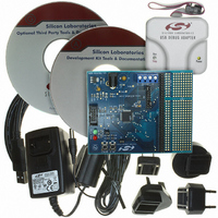
Evaluation Board, Power Supply, USB Cables, Adapter and Documentation
Processor To Be Evaluated
C8051F01x
Interface Type
USB
Silicon Manufacturer
Silicon Labs
Core Architecture
8051
Silicon Core Number
C8051F005
Silicon Family Name
C8051F00x
Lead Free Status / RoHS Status
Contains lead / RoHS non-compliant
For Use With/related Products
Silicon Laboratories C8051 F005/006/007
Lead Free Status / Rohs Status
Lead free / RoHS Compliant
Other names
336-1188
Available stocks
Company
Part Number
Manufacturer
Quantity
Price
Company:

Part Number:
C8051F005DK
Manufacturer:
SiliconL
Quantity:
1


19. TIMERS ............................................................................................................................. 138
20. PROGRAMMABLE COUNTER ARRAY..................................................................... 154
21. JTAG (IEEE 1149.1) ......................................................................................................... 164
Table 18.2. Oscillator Frequencies for Standard Baud Rates ..........................................................................136
Figure 18.8. SBUF: Serial (UART) Data Buffer Register...............................................................................136
Figure 18.9. SCON: Serial Port Control Register............................................................................................137
19.1.
Figure 19.1. T0 Mode 0 Block Diagram..........................................................................................................139
Figure 19.2. T0 Mode 2 Block Diagram..........................................................................................................140
Figure 19.3. T0 Mode 3 Block Diagram..........................................................................................................141
Figure 19.4. TCON: Timer Control Register...................................................................................................142
Figure 19.5. TMOD: Timer Mode Register.....................................................................................................143
Figure 19.6. CKCON: Clock Control Register................................................................................................144
Figure 19.7. TL0: Timer 0 Low Byte ..............................................................................................................145
Figure 19.8. TL1: Timer 1 Low Byte ..............................................................................................................145
Figure 19.9. TH0: Timer 0 High Byte .............................................................................................................145
Figure 19.10. TH1: Timer 1 High Byte ...........................................................................................................145
19.2.
Figure 19.11. T2 Mode 0 Block Diagram........................................................................................................147
Figure 19.12. T2 Mode 1 Block Diagram........................................................................................................148
Figure 19.13. T2 Mode 2 Block Diagram........................................................................................................149
Figure 19.14. T2CON: Timer 2 Control Register............................................................................................150
Figure 19.15. RCAP2L: Timer 2 Capture Register Low Byte ........................................................................151
Figure 19.16. RCAP2H: Timer 2 Capture Register High Byte .......................................................................151
Figure 19.17. TL2: Timer 2 Low Byte ............................................................................................................151
Figure 19.18. TH2: Timer 2 High Byte ...........................................................................................................151
19.3.
Figure 19.19. Timer 3 Block Diagram.............................................................................................................152
Figure 19.20. TMR3CN: Timer 3 Control Register ........................................................................................152
Figure 19.21. TMR3RLL: Timer 3 Reload Register Low Byte ......................................................................153
Figure 19.22. TMR3RLH: Timer 3 Reload Register High Byte .....................................................................153
Figure 19.23. TMR3L: Timer 3 Low Byte ......................................................................................................153
Figure 19.24. TMR3H: Timer 3 High Byte .....................................................................................................153
Figure 20.1. PCA Block Diagram ...................................................................................................................154
20.1.
Table 20.1. PCA0CPM Register Settings for PCA Capture/Compare Modules .............................................155
Figure 20.2. PCA Interrupt Block Diagram.....................................................................................................155
Figure 20.3. PCA Capture Mode Diagram ......................................................................................................156
Figure 20.4. PCA Software Timer Mode Diagram..........................................................................................157
Figure 20.5. PCA High Speed Output Mode Diagram....................................................................................157
Figure 20.6. PCA PWM Mode Diagram .........................................................................................................158
20.2.
Table 20.2. PCA Timebase Input Options.......................................................................................................159
Figure 20.7. PCA Counter/Timer Block Diagram...........................................................................................159
20.3.
Figure 20.8. PCA0CN: PCA Control Register .................................................................................................160
Figure 20.9. PCA0MD: PCA Mode Register ..................................................................................................161
Figure 20.10. PCA0CPMn: PCA Capture/Compare Registers........................................................................162
Figure 20.11. PCA0L: PCA Counter/Timer Low Byte ...................................................................................163
Figure 20.12. PCA0H: PCA Counter/Timer High Byte ..................................................................................163
Figure 20.13. PCA0CPLn: PCA Capture Module Low Byte ..........................................................................163
Figure 20.14. PCA0CPHn: PCA Capture Module High Byte.........................................................................163
Figure 21.1. IR: JTAG Instruction Register ....................................................................................................164
21.1.
Timer 0 and Timer 1 ..........................................................................................................................138
Timer 2 ..............................................................................................................................................146
Timer 3 ..............................................................................................................................................152
Capture/Compare Modules ................................................................................................................155
PCA Counter/Timer...........................................................................................................................159
Register Descriptions for PCA ..........................................................................................................160
Boundary Scan...................................................................................................................................165
Rev. 1.7
C8051F000/1/2/5/6/7
C8051F010/1/2/5/6/7
6
Related parts for C8051F005DK
Image
Part Number
Description
Manufacturer
Datasheet
Request
R

Part Number:
Description:
SMD/C°/SINGLE-ENDED OUTPUT SILICON OSCILLATOR
Manufacturer:
Silicon Laboratories Inc
Part Number:
Description:
Manufacturer:
Silicon Laboratories Inc
Datasheet:
Part Number:
Description:
N/A N/A/SI4010 AES KEYFOB DEMO WITH LCD RX
Manufacturer:
Silicon Laboratories Inc
Datasheet:
Part Number:
Description:
N/A N/A/SI4010 SIMPLIFIED KEY FOB DEMO WITH LED RX
Manufacturer:
Silicon Laboratories Inc
Datasheet:
Part Number:
Description:
N/A/-40 TO 85 OC/EZLINK MODULE; F930/4432 HIGH BAND (REV E/B1)
Manufacturer:
Silicon Laboratories Inc
Part Number:
Description:
EZLink Module; F930/4432 Low Band (rev e/B1)
Manufacturer:
Silicon Laboratories Inc
Part Number:
Description:
I°/4460 10 DBM RADIO TEST CARD 434 MHZ
Manufacturer:
Silicon Laboratories Inc
Part Number:
Description:
I°/4461 14 DBM RADIO TEST CARD 868 MHZ
Manufacturer:
Silicon Laboratories Inc
Part Number:
Description:
I°/4463 20 DBM RFSWITCH RADIO TEST CARD 460 MHZ
Manufacturer:
Silicon Laboratories Inc
Part Number:
Description:
I°/4463 20 DBM RADIO TEST CARD 868 MHZ
Manufacturer:
Silicon Laboratories Inc
Part Number:
Description:
I°/4463 27 DBM RADIO TEST CARD 868 MHZ
Manufacturer:
Silicon Laboratories Inc
Part Number:
Description:
I°/4463 SKYWORKS 30 DBM RADIO TEST CARD 915 MHZ
Manufacturer:
Silicon Laboratories Inc
Part Number:
Description:
N/A N/A/-40 TO 85 OC/4463 RFMD 30 DBM RADIO TEST CARD 915 MHZ
Manufacturer:
Silicon Laboratories Inc
Part Number:
Description:
I°/4463 20 DBM RADIO TEST CARD 169 MHZ
Manufacturer:
Silicon Laboratories Inc