C8051F005DK Silicon Laboratories Inc, C8051F005DK Datasheet - Page 8
C8051F005DK
Manufacturer Part Number
C8051F005DK
Description
DEV KIT FOR F005/006/007
Manufacturer
Silicon Laboratories Inc
Type
MCUr
Datasheet
1.C8051F005-TB.pdf
(171 pages)
Specifications of C8051F005DK
Contents
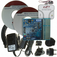
Evaluation Board, Power Supply, USB Cables, Adapter and Documentation
Processor To Be Evaluated
C8051F01x
Interface Type
USB
Silicon Manufacturer
Silicon Labs
Core Architecture
8051
Silicon Core Number
C8051F005
Silicon Family Name
C8051F00x
Lead Free Status / RoHS Status
Contains lead / RoHS non-compliant
For Use With/related Products
Silicon Laboratories C8051 F005/006/007
Lead Free Status / Rohs Status
Lead free / RoHS Compliant
Other names
336-1188
Available stocks
Company
Part Number
Manufacturer
Quantity
Price
Company:

Part Number:
C8051F005DK
Manufacturer:
SiliconL
Quantity:
1


1. SYSTEM OVERVIEW
The C8051F000 family are fully integrated mixed-signal System on a Chip MCUs with a true 12-bit multi-channel
ADC (F000/01/02/05/06/07), or a true 10-bit multi-channel ADC (F010/11/12/15/16/17). See the Product Selection
Guide in Table 1.1 for a quick reference of each MCUs’ feature set. Each has a programmable gain pre-amplifier,
two 12-bit DACs, two voltage comparators (except for the F002/07/12/17, which have one), a voltage reference,
and an 8051-compatible microcontroller core with 32kbytes of FLASH memory. There are also I2C/SMBus,
UART, and SPI serial interfaces implemented in hardware (not “bit-banged” in user software) as well as a
Programmable Counter/Timer Array (PCA) with five capture/compare modules. There are also 4 general-purpose
16-bit timers and 4 byte-wide general-purpose digital Port I/O. The C8051F000/01/02/10/11/12 have 256 bytes of
RAM and execute up to 20MIPS, while the C8051F005/06/07/15/16/17 have 2304 bytes of RAM and execute up to
25MIPS.
With an on-board VDD monitor, WDT, and clock oscillator, the MCUs are truly stand-alone System-on-a-Chip
solutions. Each MCU effectively configures and manages the analog and digital peripherals. The FLASH memory
can be reprogrammed even in-circuit, providing non-volatile data storage, and also allowing field upgrades of the
8051 firmware. Each MCU can also individually shut down any or all of the peripherals to conserve power.
On-board JTAG debug support allows non-intrusive (uses no on-chip resources), full speed, in-circuit debug using
the production MCU installed in the final application. This debug system supports inspection and modification of
memory and registers, setting breakpoints, watchpoints, single stepping, and run and halt commands. All analog
and digital peripherals are fully functional when using JTAG debug.
Each MCU is specified for 2.7V-to-3.6V operation over the industrial temperature range (-45C to +85C). The Port
I/Os, /RST, and JTAG pins are tolerant for input signals up to 5V. The C8051F000/05/10/15 are available in the
64-pin TQFP (see block diagram in Figure 1.1). The C8051F001/06/11/16 are available in the 48-pin TQFP (see
block diagram in Figure 1.2). The C8051F002/07/12/17 are available in the 32-pin LQFP (see block diagram in
Figure 1.3).
C8051F000
C8051F001
C8051F002
C8051F005
C8051F006
C8051F007
C8051F010
C8051F011
C8051F012
C8051F015
C8051F016
C8051F017
20
20
20
25
25
25
20
20
20
25
25
25
32k
32k
32k
32k
32k
32k
32k
32k
32k
32k
32k
32k
2304
2304
2304
2304
2304
2304
256
256
256
256
256
256
Table 1.1. Product Selection Guide
4
4
4
4
4
4
4
4
4
4
4
4
Rev. 1.7
32
16
32
16
32
16
32
16
8
8
8
8
12
12
12
12
12
12
10
10
10
10
10
10
100
100
100
100
100
100
100
100
100
100
100
100
C8051F000/1/2/5/6/7
C8051F010/1/2/5/6/7
8
8
4
8
8
4
8
8
4
8
8
4
12
12
12
12
12
12
12
12
12
12
12
12
2
2
2
2
2
2
2
2
2
2
2
2
2
2
1
2
2
1
2
2
1
2
2
1
64TQFP
48TQFP
32LQFP
64TQFP
48TQFP
32LQFP
64TQFP
48TQFP
32LQFP
64TQFP
48TQFP
32LQFP
8
Related parts for C8051F005DK
Image
Part Number
Description
Manufacturer
Datasheet
Request
R

Part Number:
Description:
SMD/C°/SINGLE-ENDED OUTPUT SILICON OSCILLATOR
Manufacturer:
Silicon Laboratories Inc
Part Number:
Description:
Manufacturer:
Silicon Laboratories Inc
Datasheet:
Part Number:
Description:
N/A N/A/SI4010 AES KEYFOB DEMO WITH LCD RX
Manufacturer:
Silicon Laboratories Inc
Datasheet:
Part Number:
Description:
N/A N/A/SI4010 SIMPLIFIED KEY FOB DEMO WITH LED RX
Manufacturer:
Silicon Laboratories Inc
Datasheet:
Part Number:
Description:
N/A/-40 TO 85 OC/EZLINK MODULE; F930/4432 HIGH BAND (REV E/B1)
Manufacturer:
Silicon Laboratories Inc
Part Number:
Description:
EZLink Module; F930/4432 Low Band (rev e/B1)
Manufacturer:
Silicon Laboratories Inc
Part Number:
Description:
I°/4460 10 DBM RADIO TEST CARD 434 MHZ
Manufacturer:
Silicon Laboratories Inc
Part Number:
Description:
I°/4461 14 DBM RADIO TEST CARD 868 MHZ
Manufacturer:
Silicon Laboratories Inc
Part Number:
Description:
I°/4463 20 DBM RFSWITCH RADIO TEST CARD 460 MHZ
Manufacturer:
Silicon Laboratories Inc
Part Number:
Description:
I°/4463 20 DBM RADIO TEST CARD 868 MHZ
Manufacturer:
Silicon Laboratories Inc
Part Number:
Description:
I°/4463 27 DBM RADIO TEST CARD 868 MHZ
Manufacturer:
Silicon Laboratories Inc
Part Number:
Description:
I°/4463 SKYWORKS 30 DBM RADIO TEST CARD 915 MHZ
Manufacturer:
Silicon Laboratories Inc
Part Number:
Description:
N/A N/A/-40 TO 85 OC/4463 RFMD 30 DBM RADIO TEST CARD 915 MHZ
Manufacturer:
Silicon Laboratories Inc
Part Number:
Description:
I°/4463 20 DBM RADIO TEST CARD 169 MHZ
Manufacturer:
Silicon Laboratories Inc