C8051F410DK Silicon Laboratories Inc, C8051F410DK Datasheet - Page 131
C8051F410DK
Manufacturer Part Number
C8051F410DK
Description
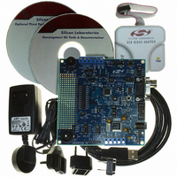
KIT DEV FOR C8051F41X
Manufacturer
Silicon Laboratories Inc
Type
MCUr
Specifications of C8051F410DK
Contents
Evaluation Board, Power Supply, USB Cables, Adapter and Documentation
Processor To Be Evaluated
C8051F41x
Interface Type
USB
Silicon Manufacturer
Silicon Labs
Core Architecture
8051
Silicon Core Number
C8051F410
Silicon Family Name
C8051F41x
Lead Free Status / RoHS Status
Contains lead / RoHS non-compliant
For Use With/related Products
Silicon Laboratories C8051F41x
Lead Free Status / Rohs Status
Lead free / RoHS Compliant
Other names
336-1314
Available stocks
Company
Part Number
Manufacturer
Quantity
Price
Company:

Part Number:
C8051F410DK
Manufacturer:
Silicon Labs
Quantity:
135


inverting input voltage (on CP0+) is less than the inverting input voltage (on CP0-), the device is put into
the reset state. After a Comparator0 reset, the C0RSEF flag (RSTSRC.5) will read ‘1’ signifying
Comparator0 as the reset source; otherwise, this bit reads ‘0’. The state of the RST pin is unaffected by
this reset.
15.6. PCA Watchdog Timer Reset
The programmable Watchdog Timer (WDT) function of the Programmable Counter Array (PCA) can be
used to prevent software from running out of control during a system malfunction. The PCA WDT function
can be enabled or disabled by software as described in
page 257
prevents user software from updating the WDT, a reset is generated and the WDTRSF bit (RSTSRC.5) is
set to ‘1’. The state of the RST pin is unaffected by this reset.
15.7. Flash Error Reset
If a Flash read/write/erase or program read targets an illegal address, a system reset is generated. This
may occur due to any of the following:
•
•
•
•
•
The FERROR bit (RSTSRC.6) is set following a Flash error reset. The state of the RST pin is unaffected by
this reset.
A Flash write or erase is attempted above user code space. This occurs when PSWE is set to ‘1’ and a
MOVX write operation targets an address above the Lock Byte address.
A Flash read is attempted above user code space. This occurs when a MOVC operation targets an
address above the Lock Byte address.
A Program read is attempted above user code space. This occurs when user code attempts to branch
to an address above the Lock Byte address.
A Flash read, write or erase attempt is restricted due to a Flash security setting (see
“16.3. Security Options” on page 137
A Flash write or erase is attempted while the V
; the WDT is enabled and clocked by SYSCLK / 12 following any reset. If a system malfunction
).
Rev. 1.1
DD
Monitor is disabled.
Section “25.3. Watchdog Timer Mode” on
C8051F410/1/2/3
Section
131
Related parts for C8051F410DK
Image
Part Number
Description
Manufacturer
Datasheet
Request
R

Part Number:
Description:
SMD/C°/SINGLE-ENDED OUTPUT SILICON OSCILLATOR
Manufacturer:
Silicon Laboratories Inc
Part Number:
Description:
Manufacturer:
Silicon Laboratories Inc
Datasheet:
Part Number:
Description:
N/A N/A/SI4010 AES KEYFOB DEMO WITH LCD RX
Manufacturer:
Silicon Laboratories Inc
Datasheet:
Part Number:
Description:
N/A N/A/SI4010 SIMPLIFIED KEY FOB DEMO WITH LED RX
Manufacturer:
Silicon Laboratories Inc
Datasheet:
Part Number:
Description:
N/A/-40 TO 85 OC/EZLINK MODULE; F930/4432 HIGH BAND (REV E/B1)
Manufacturer:
Silicon Laboratories Inc
Part Number:
Description:
EZLink Module; F930/4432 Low Band (rev e/B1)
Manufacturer:
Silicon Laboratories Inc
Part Number:
Description:
I°/4460 10 DBM RADIO TEST CARD 434 MHZ
Manufacturer:
Silicon Laboratories Inc
Part Number:
Description:
I°/4461 14 DBM RADIO TEST CARD 868 MHZ
Manufacturer:
Silicon Laboratories Inc
Part Number:
Description:
I°/4463 20 DBM RFSWITCH RADIO TEST CARD 460 MHZ
Manufacturer:
Silicon Laboratories Inc
Part Number:
Description:
I°/4463 20 DBM RADIO TEST CARD 868 MHZ
Manufacturer:
Silicon Laboratories Inc
Part Number:
Description:
I°/4463 27 DBM RADIO TEST CARD 868 MHZ
Manufacturer:
Silicon Laboratories Inc
Part Number:
Description:
I°/4463 SKYWORKS 30 DBM RADIO TEST CARD 915 MHZ
Manufacturer:
Silicon Laboratories Inc
Part Number:
Description:
N/A N/A/-40 TO 85 OC/4463 RFMD 30 DBM RADIO TEST CARD 915 MHZ
Manufacturer:
Silicon Laboratories Inc
Part Number:
Description:
I°/4463 20 DBM RADIO TEST CARD 169 MHZ
Manufacturer:
Silicon Laboratories Inc