C8051F410DK Silicon Laboratories Inc, C8051F410DK Datasheet - Page 155
C8051F410DK
Manufacturer Part Number
C8051F410DK
Description
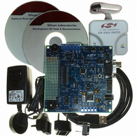
KIT DEV FOR C8051F41X
Manufacturer
Silicon Laboratories Inc
Type
MCUr
Specifications of C8051F410DK
Contents
Evaluation Board, Power Supply, USB Cables, Adapter and Documentation
Processor To Be Evaluated
C8051F41x
Interface Type
USB
Silicon Manufacturer
Silicon Labs
Core Architecture
8051
Silicon Core Number
C8051F410
Silicon Family Name
C8051F41x
Lead Free Status / RoHS Status
Contains lead / RoHS non-compliant
For Use With/related Products
Silicon Laboratories C8051F41x
Lead Free Status / Rohs Status
Lead free / RoHS Compliant
Other names
336-1314
Available stocks
Company
Part Number
Manufacturer
Quantity
Price
Company:

Part Number:
C8051F410DK
Manufacturer:
Silicon Labs
Quantity:
135


(P1MATCH & P1MASK). This allows Software to be notified if a certain change or pattern occurs on P0 or
P1 input pins regardless of the XBRn settings. A port match event can cause an interrupt if EMAT (EIE2.1)
is set to '1' or cause the internal oscillator to awaken from SUSPEND mode. See Section “
Oscillator Suspend Mode
Bits7–0: P0.[7:0]
Bits7–0: Analog Input Configuration Bits for P0.7–P0.0 (respectively).
P0.7
R/W
R/W
Bit7
Bit7
Write - Output appears on I/O pins per Crossbar Registers.
0: Logic Low Output.
1: Logic High Output (high impedance if corresponding P0MDOUT.n bit = 0).
Read - Always reads ‘0’ if selected as analog input in register P0MDIN. Directly reads Port
pin when configured as digital input.
0: P0.n pin is logic low.
1: P0.n pin is logic high.
Port pins configured as analog inputs have their weak pullup, digital driver, and digital
receiver disabled.
0: Corresponding P0.n pin is configured as an analog input. In order for the P0.n pin to be
in analog input mode, there MUST be a '1' in the Port Latch register corresponding to
that pin.
1: Corresponding P0.n pin is not configured as an analog input.
P0.6
R/W
R/W
Bit6
Bit6
SFR Definition 18.4. P0MDIN: Port0 Input Mode
” on page
P0.5
R/W
R/W
Bit5
Bit5
SFR Definition 18.3. P0: Port0
166
P0.4
R/W
R/W
Bit4
Bit4
for more information.
Rev. 1.1
P0.3
R/W
R/W
Bit3
Bit3
P0.2
R/W
R/W
Bit2
Bit2
C8051F410/1/2/3
P0.1
R/W
R/W
Bit1
Bit1
SFR Address:
SFR Address:
P0.0
R/W
R/W
Bit0
Bit0
19.1.1. Internal
0xF1
0x80
Addressable
Reset Value
Reset Value
11111111
11111111
Bit
155
Related parts for C8051F410DK
Image
Part Number
Description
Manufacturer
Datasheet
Request
R

Part Number:
Description:
SMD/C°/SINGLE-ENDED OUTPUT SILICON OSCILLATOR
Manufacturer:
Silicon Laboratories Inc
Part Number:
Description:
Manufacturer:
Silicon Laboratories Inc
Datasheet:
Part Number:
Description:
N/A N/A/SI4010 AES KEYFOB DEMO WITH LCD RX
Manufacturer:
Silicon Laboratories Inc
Datasheet:
Part Number:
Description:
N/A N/A/SI4010 SIMPLIFIED KEY FOB DEMO WITH LED RX
Manufacturer:
Silicon Laboratories Inc
Datasheet:
Part Number:
Description:
N/A/-40 TO 85 OC/EZLINK MODULE; F930/4432 HIGH BAND (REV E/B1)
Manufacturer:
Silicon Laboratories Inc
Part Number:
Description:
EZLink Module; F930/4432 Low Band (rev e/B1)
Manufacturer:
Silicon Laboratories Inc
Part Number:
Description:
I°/4460 10 DBM RADIO TEST CARD 434 MHZ
Manufacturer:
Silicon Laboratories Inc
Part Number:
Description:
I°/4461 14 DBM RADIO TEST CARD 868 MHZ
Manufacturer:
Silicon Laboratories Inc
Part Number:
Description:
I°/4463 20 DBM RFSWITCH RADIO TEST CARD 460 MHZ
Manufacturer:
Silicon Laboratories Inc
Part Number:
Description:
I°/4463 20 DBM RADIO TEST CARD 868 MHZ
Manufacturer:
Silicon Laboratories Inc
Part Number:
Description:
I°/4463 27 DBM RADIO TEST CARD 868 MHZ
Manufacturer:
Silicon Laboratories Inc
Part Number:
Description:
I°/4463 SKYWORKS 30 DBM RADIO TEST CARD 915 MHZ
Manufacturer:
Silicon Laboratories Inc
Part Number:
Description:
N/A N/A/-40 TO 85 OC/4463 RFMD 30 DBM RADIO TEST CARD 915 MHZ
Manufacturer:
Silicon Laboratories Inc
Part Number:
Description:
I°/4463 20 DBM RADIO TEST CARD 169 MHZ
Manufacturer:
Silicon Laboratories Inc