C8051F410DK Silicon Laboratories Inc, C8051F410DK Datasheet - Page 181
C8051F410DK
Manufacturer Part Number
C8051F410DK
Description
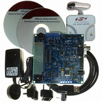
KIT DEV FOR C8051F41X
Manufacturer
Silicon Laboratories Inc
Type
MCUr
Specifications of C8051F410DK
Contents
Evaluation Board, Power Supply, USB Cables, Adapter and Documentation
Processor To Be Evaluated
C8051F41x
Interface Type
USB
Silicon Manufacturer
Silicon Labs
Core Architecture
8051
Silicon Core Number
C8051F410
Silicon Family Name
C8051F41x
Lead Free Status / RoHS Status
Contains lead / RoHS non-compliant
For Use With/related Products
Silicon Laboratories C8051F41x
Lead Free Status / Rohs Status
Lead free / RoHS Compliant
Other names
336-1314
Available stocks
Company
Part Number
Manufacturer
Quantity
Price
Company:

Part Number:
C8051F410DK
Manufacturer:
Silicon Labs
Quantity:
135


Bit 7:
Bit 6:
Bit 5:
Bit 4:
Bits 3–0: RTC0ADDR: smaRTClock Address Bits
BUSY
R/W
Bit7
BUSY: smaRTClock Interface Busy bit.
Writing a ‘1’ to this bit initiates a smaRTClock indirect read operation. This bit is automati-
cally cleared by hardware when the operation is complete.
0: smaRTClock Interface is not busy.
1: smaRTClock Interface is busy performing a read or write operation.
AUTORD: smaRTClock Interface Auto Read Enable.
0: BUSY must be written manually for each smaRTClock indirect read operation.
1: The next smaRTClock indirect read operation is initiated when RTC0DAT is read by soft-
ware.
VREGEN: Backup Supply Voltage Regulator Enable.
This bit is automatically set to 1b when V
0: Backup Supply Voltage Regulator Disabled (smaRTClock powered from V
1: Force Backup Supply Voltage Regulator Enabled (smaRTClock powered from V
BACKUP
SHORT: Short Read/Write Timing Enable.
0: smaRTClock reads and writes are 4 system clocks wide.
1: smaRTClock reads and writes are 1 system clock wide.
Note: Increasing the speed of the smaRTClock reads and writes may also slightly increase
power consumption.
These bits select the smaRTClock internal register that is targeted by reads/writes to
RTC0DAT.
Note: The RTC0ADDR bits increment after each indirect read/write operation that
targets a CAPTUREn or ALARMn internal register.
AUTORD VREGEN
RTC0ADDR
R/W
Bit6
SFR Definition 20.2. RTC0ADR: smaRTClock Address
).
0000
0001
0010
0100
0101
1000
1001
1010
0011
0110
0111
1011
1100
1101
1110
1111
R/W
Bit5
smaRTClock Internal Register
SHORT
R/W
Bit4
CAPTURE0
CAPTURE1
CAPTURE2
CAPTURE3
CAPTURE4
CAPTURE5
RAMADDR
RTC0XCN
RAMDATA
RTC0CN
ALARM0
ALARM1
ALARM2
ALARM3
ALARM4
ALARM5
Rev. 1.1
R/W
Bit3
RTC-BACKUP
R/W
Bit2
RTC0ADDR
> V
DD
C8051F410/1/2/3
.
R/W
Bit1
SFR Address:
R/W
Bit0
DD
).
0xAC
Reset Value
RTC-
Variable
181
Related parts for C8051F410DK
Image
Part Number
Description
Manufacturer
Datasheet
Request
R

Part Number:
Description:
SMD/C°/SINGLE-ENDED OUTPUT SILICON OSCILLATOR
Manufacturer:
Silicon Laboratories Inc
Part Number:
Description:
Manufacturer:
Silicon Laboratories Inc
Datasheet:
Part Number:
Description:
N/A N/A/SI4010 AES KEYFOB DEMO WITH LCD RX
Manufacturer:
Silicon Laboratories Inc
Datasheet:
Part Number:
Description:
N/A N/A/SI4010 SIMPLIFIED KEY FOB DEMO WITH LED RX
Manufacturer:
Silicon Laboratories Inc
Datasheet:
Part Number:
Description:
N/A/-40 TO 85 OC/EZLINK MODULE; F930/4432 HIGH BAND (REV E/B1)
Manufacturer:
Silicon Laboratories Inc
Part Number:
Description:
EZLink Module; F930/4432 Low Band (rev e/B1)
Manufacturer:
Silicon Laboratories Inc
Part Number:
Description:
I°/4460 10 DBM RADIO TEST CARD 434 MHZ
Manufacturer:
Silicon Laboratories Inc
Part Number:
Description:
I°/4461 14 DBM RADIO TEST CARD 868 MHZ
Manufacturer:
Silicon Laboratories Inc
Part Number:
Description:
I°/4463 20 DBM RFSWITCH RADIO TEST CARD 460 MHZ
Manufacturer:
Silicon Laboratories Inc
Part Number:
Description:
I°/4463 20 DBM RADIO TEST CARD 868 MHZ
Manufacturer:
Silicon Laboratories Inc
Part Number:
Description:
I°/4463 27 DBM RADIO TEST CARD 868 MHZ
Manufacturer:
Silicon Laboratories Inc
Part Number:
Description:
I°/4463 SKYWORKS 30 DBM RADIO TEST CARD 915 MHZ
Manufacturer:
Silicon Laboratories Inc
Part Number:
Description:
N/A N/A/-40 TO 85 OC/4463 RFMD 30 DBM RADIO TEST CARD 915 MHZ
Manufacturer:
Silicon Laboratories Inc
Part Number:
Description:
I°/4463 20 DBM RADIO TEST CARD 169 MHZ
Manufacturer:
Silicon Laboratories Inc