C8051F410DK Silicon Laboratories Inc, C8051F410DK Datasheet - Page 234
C8051F410DK
Manufacturer Part Number
C8051F410DK
Description
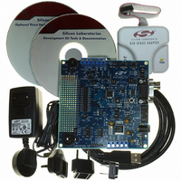
KIT DEV FOR C8051F41X
Manufacturer
Silicon Laboratories Inc
Type
MCUr
Specifications of C8051F410DK
Contents
Evaluation Board, Power Supply, USB Cables, Adapter and Documentation
Processor To Be Evaluated
C8051F41x
Interface Type
USB
Silicon Manufacturer
Silicon Labs
Core Architecture
8051
Silicon Core Number
C8051F410
Silicon Family Name
C8051F41x
Lead Free Status / RoHS Status
Contains lead / RoHS non-compliant
For Use With/related Products
Silicon Laboratories C8051F41x
Lead Free Status / Rohs Status
Lead free / RoHS Compliant
Other names
336-1314
Available stocks
Company
Part Number
Manufacturer
Quantity
Price
Company:

Part Number:
C8051F410DK
Manufacturer:
Silicon Labs
Quantity:
135


C8051F410/1/2/3
24.1.4. Mode 3: Two 8-bit Counter/Timers (Timer 0 Only)
In Mode 3, Timer 0 is configured as two separate 8-bit counter/timers held in TL0 and TH0. The coun-
ter/timer in TL0 is controlled using the Timer 0 control/status bits in TCON and TMOD: TR0, C/T0, GATE0
and TF0. TL0 can use either the system clock or an external input signal as its timebase. The TH0 register
is restricted to a timer function sourced by the system clock or prescaled clock. TH0 is enabled using the
Timer 1 run control bit TR1. TH0 sets the Timer 1 overflow flag TF1 on overflow and thus controls the
Timer 1 interrupt.
Timer 1 is inactive in Mode 3. When Timer 0 is operating in Mode 3, Timer 1 can be operated in Modes 0,
1 or 2, but cannot be clocked by external signals nor set the TF1 flag and generate an interrupt. However,
the Timer 1 overflow can be used to generate baud rates for the SMBus and UART. While Timer 0 is oper-
ating in Mode 3, Timer 1 run control is handled through its mode settings. To run Timer 1 while Timer 0 is in
Mode 3, set the Timer 1 Mode as 0, 1, or 2. To disable Timer 1, configure it for Mode 3.
234
/INT0
T0
Crossbar
Pre-scaled Clock
SYSCLK
IN0PL
GATE0
Figure 24.3. T0 Mode 3 Block Diagram
XOR
0
1
TR0
M
T
3
H
M
T
3
L
CKCON
M
H
T
2
0
1
M
T
2
L
M
T
1
M
T
0
S
C
A
1
S
C
A
0
Rev. 1.1
TR1
G
A
T
E
1
C
T
1
/
M
T
1
1
TMOD
M
T
1
0
G
A
T
E
0
C
T
0
/
M
T
0
1
M
T
0
0
(8 bits)
(8 bits)
TH0
TL0
TR1
TR0
TF1
TF0
IE1
IE0
IT1
IT0
Interrupt
Interrupt
Related parts for C8051F410DK
Image
Part Number
Description
Manufacturer
Datasheet
Request
R

Part Number:
Description:
SMD/C°/SINGLE-ENDED OUTPUT SILICON OSCILLATOR
Manufacturer:
Silicon Laboratories Inc
Part Number:
Description:
Manufacturer:
Silicon Laboratories Inc
Datasheet:
Part Number:
Description:
N/A N/A/SI4010 AES KEYFOB DEMO WITH LCD RX
Manufacturer:
Silicon Laboratories Inc
Datasheet:
Part Number:
Description:
N/A N/A/SI4010 SIMPLIFIED KEY FOB DEMO WITH LED RX
Manufacturer:
Silicon Laboratories Inc
Datasheet:
Part Number:
Description:
N/A/-40 TO 85 OC/EZLINK MODULE; F930/4432 HIGH BAND (REV E/B1)
Manufacturer:
Silicon Laboratories Inc
Part Number:
Description:
EZLink Module; F930/4432 Low Band (rev e/B1)
Manufacturer:
Silicon Laboratories Inc
Part Number:
Description:
I°/4460 10 DBM RADIO TEST CARD 434 MHZ
Manufacturer:
Silicon Laboratories Inc
Part Number:
Description:
I°/4461 14 DBM RADIO TEST CARD 868 MHZ
Manufacturer:
Silicon Laboratories Inc
Part Number:
Description:
I°/4463 20 DBM RFSWITCH RADIO TEST CARD 460 MHZ
Manufacturer:
Silicon Laboratories Inc
Part Number:
Description:
I°/4463 20 DBM RADIO TEST CARD 868 MHZ
Manufacturer:
Silicon Laboratories Inc
Part Number:
Description:
I°/4463 27 DBM RADIO TEST CARD 868 MHZ
Manufacturer:
Silicon Laboratories Inc
Part Number:
Description:
I°/4463 SKYWORKS 30 DBM RADIO TEST CARD 915 MHZ
Manufacturer:
Silicon Laboratories Inc
Part Number:
Description:
N/A N/A/-40 TO 85 OC/4463 RFMD 30 DBM RADIO TEST CARD 915 MHZ
Manufacturer:
Silicon Laboratories Inc
Part Number:
Description:
I°/4463 20 DBM RADIO TEST CARD 169 MHZ
Manufacturer:
Silicon Laboratories Inc