C8051F410DK Silicon Laboratories Inc, C8051F410DK Datasheet - Page 54
C8051F410DK
Manufacturer Part Number
C8051F410DK
Description
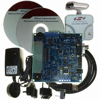
KIT DEV FOR C8051F41X
Manufacturer
Silicon Laboratories Inc
Type
MCUr
Specifications of C8051F410DK
Contents
Evaluation Board, Power Supply, USB Cables, Adapter and Documentation
Processor To Be Evaluated
C8051F41x
Interface Type
USB
Silicon Manufacturer
Silicon Labs
Core Architecture
8051
Silicon Core Number
C8051F410
Silicon Family Name
C8051F41x
Lead Free Status / RoHS Status
Contains lead / RoHS non-compliant
For Use With/related Products
Silicon Laboratories C8051F41x
Lead Free Status / Rohs Status
Lead free / RoHS Compliant
Other names
336-1314
Available stocks
Company
Part Number
Manufacturer
Quantity
Price
Company:

Part Number:
C8051F410DK
Manufacturer:
Silicon Labs
Quantity:
135


C8051F410/1/2/3
Depending on the output connected to the ADC input, additional tracking time, more than is specified in
Table 5.3 and Table 5.4, may be required after changing MUX settings. See the settling time requirements
described in
5.3.3. Timing
ADC0 has a maximum conversion speed specified in Table 5.3 and Table 5.4. ADC0 is clocked from the
ADC0 Subsystem Clock (FCLK). The source of FCLK is selected based on the BURSTEN bit. When
BURSTEN is logic 0, FCLK is derived from the current system clock. When BURSTEN is logic 1, FCLK is
derived from the Burst Mode Oscillator, an independent clock source with a maximum frequency of
25 MHz.
When ADC0 is performing a conversion, it requires a clock source that is typically slower than FCLK. The
ADC0 SAR conversion clock (SAR clock) is a divided version of FCLK. The divide ratio can be configured
using the AD0SC bits in the ADC0CF register. The maximum SAR clock frequency is listed in Table 5.3
and Table 5.4.
ADC0 can be in one of three states at any given time: tracking, converting, or idle. Tracking time depends
on the tracking mode selected. For Pre-Tracking Mode, tracking is managed by software and ADC0 starts
conversions immediately following the convert start signal. For Post-Tracking and Dual-Tracking Modes,
the tracking time after the convert start signal is equal to the value determined by the AD0TK bits plus 2
FCLK cycles. Tracking is immediately followed by a conversion. The ADC0 conversion time is always 13
SAR clock cycles plus an additional 2 FCLK cycles to start and complete a conversion. Figure 5.4 shows
timing diagrams for a conversion in Pre-Tracking Mode and tracking plus conversion in Post-Tracking or
Dual-Tracking Mode. In this example, repeat count is set to one.
54
Dual-Tracking
Post-Tracking
Convert Start
Pre-Tracking
AD0TM = 10
AD0TM = 11
AD0TM= 01
Section “5.3.6. Settling Time Requirements” on page 58
Track
Track
Idle
Track
Track
Figure 5.3. ADC0 Tracking Modes
Convert
Rev. 1.1
Convert
Convert
Track
.
Track
Idle
Track
Track
Convert ...
Convert..
Convert..
Related parts for C8051F410DK
Image
Part Number
Description
Manufacturer
Datasheet
Request
R

Part Number:
Description:
SMD/C°/SINGLE-ENDED OUTPUT SILICON OSCILLATOR
Manufacturer:
Silicon Laboratories Inc
Part Number:
Description:
Manufacturer:
Silicon Laboratories Inc
Datasheet:
Part Number:
Description:
N/A N/A/SI4010 AES KEYFOB DEMO WITH LCD RX
Manufacturer:
Silicon Laboratories Inc
Datasheet:
Part Number:
Description:
N/A N/A/SI4010 SIMPLIFIED KEY FOB DEMO WITH LED RX
Manufacturer:
Silicon Laboratories Inc
Datasheet:
Part Number:
Description:
N/A/-40 TO 85 OC/EZLINK MODULE; F930/4432 HIGH BAND (REV E/B1)
Manufacturer:
Silicon Laboratories Inc
Part Number:
Description:
EZLink Module; F930/4432 Low Band (rev e/B1)
Manufacturer:
Silicon Laboratories Inc
Part Number:
Description:
I°/4460 10 DBM RADIO TEST CARD 434 MHZ
Manufacturer:
Silicon Laboratories Inc
Part Number:
Description:
I°/4461 14 DBM RADIO TEST CARD 868 MHZ
Manufacturer:
Silicon Laboratories Inc
Part Number:
Description:
I°/4463 20 DBM RFSWITCH RADIO TEST CARD 460 MHZ
Manufacturer:
Silicon Laboratories Inc
Part Number:
Description:
I°/4463 20 DBM RADIO TEST CARD 868 MHZ
Manufacturer:
Silicon Laboratories Inc
Part Number:
Description:
I°/4463 27 DBM RADIO TEST CARD 868 MHZ
Manufacturer:
Silicon Laboratories Inc
Part Number:
Description:
I°/4463 SKYWORKS 30 DBM RADIO TEST CARD 915 MHZ
Manufacturer:
Silicon Laboratories Inc
Part Number:
Description:
N/A N/A/-40 TO 85 OC/4463 RFMD 30 DBM RADIO TEST CARD 915 MHZ
Manufacturer:
Silicon Laboratories Inc
Part Number:
Description:
I°/4463 20 DBM RADIO TEST CARD 169 MHZ
Manufacturer:
Silicon Laboratories Inc