C8051F410DK Silicon Laboratories Inc, C8051F410DK Datasheet - Page 85
C8051F410DK
Manufacturer Part Number
C8051F410DK
Description
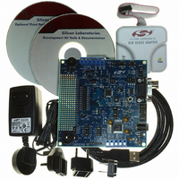
KIT DEV FOR C8051F41X
Manufacturer
Silicon Laboratories Inc
Type
MCUr
Specifications of C8051F410DK
Contents
Evaluation Board, Power Supply, USB Cables, Adapter and Documentation
Processor To Be Evaluated
C8051F41x
Interface Type
USB
Silicon Manufacturer
Silicon Labs
Core Architecture
8051
Silicon Core Number
C8051F410
Silicon Family Name
C8051F41x
Lead Free Status / RoHS Status
Contains lead / RoHS non-compliant
For Use With/related Products
Silicon Laboratories C8051F41x
Lead Free Status / Rohs Status
Lead free / RoHS Compliant
Other names
336-1314
Available stocks
Company
Part Number
Manufacturer
Quantity
Price
Company:

Part Number:
C8051F410DK
Manufacturer:
Silicon Labs
Quantity:
135


The Comparator hysteresis is software-programmable via its Comparator Control register CPTnCN (for
n = 0 or 1). The user can program both the amount of hysteresis voltage (referred to the input voltage) and
the positive and negative-going symmetry of this hysteresis around the threshold voltage.
The Comparator hysteresis is programmed using Bits3-0 in the Comparator Control Register CPTnCN
(shown in SFR Definition 9.1 and SFR Definition 9.6). The amount of negative hysteresis voltage is
determined by the settings of the CPnHYN bits. As shown in Table 9.1, settings of 20, 10 or 5 mV of
negative hysteresis can be programmed, or negative hysteresis can be disabled. In a similar way, the
amount of positive hysteresis is determined by setting the CPnHYP bits.
Comparator interrupts can be generated on both rising-edge and falling-edge output transitions. (For Inter-
rupt enable and priority control, see
set to logic 1 upon a Comparator falling-edge detect, and the CPnRIF flag is set to logic 1 upon the Com-
parator rising-edge detect. Once set, these bits remain set until cleared by software. The output state of
the Comparator can be obtained at any time by reading the CPnOUT bit. The Comparator is enabled by
setting the CPnEN bit to logic 1, and is disabled by clearing this bit to logic 0.
The output state of the Comparator can be obtained at any time by reading the CPnOUT bit. The Compar-
ator is enabled by setting the CPnEN bit to logic 1, and is disabled by clearing this bit to logic 0. When the
Comparator is enabled, the internal oscillator is awakened from SUSPEND mode if the Comparator output
is logic 0.
Note that false rising edges and falling edges can be detected when the comparator is first powered-on or
if changes are made to the hysteresis or response time control bits. Therefore, it is recommended that the
rising-edge and falling-edge flags be explicitly cleared to logic 0 a short time after the comparator is
enabled or its mode bits have been changed. This Power Up Time is specified in Table 9.1 on page 92.
(Programmed with CP0HYP Bits)
Positive Hysteresis Voltage
INPUTS
OUTPUT
VIN+
VIN-
CIRCUIT CONFIGURATION
Positive Hysteresis
CP0-
VIN+
CP0+
VIN-
V
Disabled
Figure 9.3. Comparator Hysteresis Plot
OL
V
OH
+
_
CP0
Section “12. Interrupt Handler” on page 110
Positive Hysteresis
Maximum
OUT
Rev. 1.1
Negative Hysteresis
Disabled
Negative Hysteresis
C8051F410/1/2/3
(Programmed by CP0HYN Bits)
Maximum
Negative Hysteresis Voltage
). The CPnFIF flag is
85
Related parts for C8051F410DK
Image
Part Number
Description
Manufacturer
Datasheet
Request
R

Part Number:
Description:
SMD/C°/SINGLE-ENDED OUTPUT SILICON OSCILLATOR
Manufacturer:
Silicon Laboratories Inc
Part Number:
Description:
Manufacturer:
Silicon Laboratories Inc
Datasheet:
Part Number:
Description:
N/A N/A/SI4010 AES KEYFOB DEMO WITH LCD RX
Manufacturer:
Silicon Laboratories Inc
Datasheet:
Part Number:
Description:
N/A N/A/SI4010 SIMPLIFIED KEY FOB DEMO WITH LED RX
Manufacturer:
Silicon Laboratories Inc
Datasheet:
Part Number:
Description:
N/A/-40 TO 85 OC/EZLINK MODULE; F930/4432 HIGH BAND (REV E/B1)
Manufacturer:
Silicon Laboratories Inc
Part Number:
Description:
EZLink Module; F930/4432 Low Band (rev e/B1)
Manufacturer:
Silicon Laboratories Inc
Part Number:
Description:
I°/4460 10 DBM RADIO TEST CARD 434 MHZ
Manufacturer:
Silicon Laboratories Inc
Part Number:
Description:
I°/4461 14 DBM RADIO TEST CARD 868 MHZ
Manufacturer:
Silicon Laboratories Inc
Part Number:
Description:
I°/4463 20 DBM RFSWITCH RADIO TEST CARD 460 MHZ
Manufacturer:
Silicon Laboratories Inc
Part Number:
Description:
I°/4463 20 DBM RADIO TEST CARD 868 MHZ
Manufacturer:
Silicon Laboratories Inc
Part Number:
Description:
I°/4463 27 DBM RADIO TEST CARD 868 MHZ
Manufacturer:
Silicon Laboratories Inc
Part Number:
Description:
I°/4463 SKYWORKS 30 DBM RADIO TEST CARD 915 MHZ
Manufacturer:
Silicon Laboratories Inc
Part Number:
Description:
N/A N/A/-40 TO 85 OC/4463 RFMD 30 DBM RADIO TEST CARD 915 MHZ
Manufacturer:
Silicon Laboratories Inc
Part Number:
Description:
I°/4463 20 DBM RADIO TEST CARD 169 MHZ
Manufacturer:
Silicon Laboratories Inc