R0K561622S000BE Renesas Electronics America, R0K561622S000BE Datasheet - Page 35
R0K561622S000BE
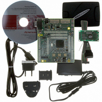
Manufacturer Part Number
R0K561622S000BE
Description
KIT STARTER FOR H8SX/1622
Manufacturer
Renesas Electronics America
Series
Renesas Starter Kits (RSK)r
Type
MCUr
Specifications of R0K561622S000BE
Contents
Board, Cables, CD, Debugger, Power Supply
Silicon Manufacturer
Renesas
Features
Coding And Debugging, E10A Emulator, RS232 Serial Connection
Kit Contents
Board
Silicon Family Name
H8SX/1622F
Silicon Core Number
R5F61622N50LGV
Lead Free Status / RoHS Status
Lead free / RoHS Compliant
For Use With/related Products
H8SX/1622
Lead Free Status / RoHS Status
Lead free / RoHS Compliant, Lead free / RoHS Compliant


Classification
Clock
A/D converter
Module/
Function
Clock pulse
generator
(CPG)
10-bit A/D
converter
(ADC)
16-bit
∆Σ A/D
converter
(∆Σ AD)
Description
•
•
•
•
•
•
•
•
•
•
•
•
•
•
•
•
One clock generation circuit available
Separate clock signals are provided for each of functional
modules (detailed below) and each is independently specifiable
(multi-clock function)
System-intended data transfer modules, i.e. the CPU, are
On-chip peripheral functions are run by the peripheral
External space modules are supplied with the external bus
∆Σ A/D converter is run by the clock for ∆Σ A/D converter
Includes a PLL frequency multiplier and frequency dividers
(including a divider for Aφ), so the operating frequency is
selectable
Five power-down modes: Sleep mode, all-module-clock-stop
mode, software standby mode, deep software standby mode,
and hardware standby mode
10-bit resolution × eight input channels
Sample and hold function included
Conversion time: 5.33 µs per channel (with ADCLK at 7.5 MHz
operation)
Two operating modes: single mode and scan mode
Three ways to start A/D conversion: by software, timer
(TPU/TMR) trigger, and external trigger
(Starting by TPU/TMR: This operation is available on the on-chip
emulator but not available on other emulators.)
16-bit resolution
Six input channels (differential inputs on two channels)
Conversion time: 286 states
Two operating modes: single mode and scan mode
∆Σ modulation
Three ways to start A/D conversion: by software, timer
(TPU/TMR) trigger, and external trigger
(Starting by TPU/TMR: This operation is available on the on-chip
emulator but not available on other emulators.)
Input voltage offset cancellation in two modes: by register setting
and by differential input
run by the system clock (Iφ): 8 to 50 MHz
module clock (Pφ): 8 to 35 MHz
clock (Bφ): 8 to 50 MHz
(Aφ): near 25 MHz
Rev. 2.00 Sep. 16, 2009 Page 5 of 1036
Section 1 Overview
REJ09B0414-0200
Related parts for R0K561622S000BE
Image
Part Number
Description
Manufacturer
Datasheet
Request
R

Part Number:
Description:
KIT STARTER FOR M16C/29
Manufacturer:
Renesas Electronics America
Datasheet:

Part Number:
Description:
KIT STARTER FOR R8C/2D
Manufacturer:
Renesas Electronics America
Datasheet:

Part Number:
Description:
R0K33062P STARTER KIT
Manufacturer:
Renesas Electronics America
Datasheet:

Part Number:
Description:
KIT STARTER FOR R8C/23 E8A
Manufacturer:
Renesas Electronics America
Datasheet:

Part Number:
Description:
KIT STARTER FOR R8C/25
Manufacturer:
Renesas Electronics America
Datasheet:

Part Number:
Description:
KIT STARTER H8S2456 SHARPE DSPLY
Manufacturer:
Renesas Electronics America
Datasheet:

Part Number:
Description:
KIT STARTER FOR R8C38C
Manufacturer:
Renesas Electronics America
Datasheet:

Part Number:
Description:
KIT STARTER FOR R8C35C
Manufacturer:
Renesas Electronics America
Datasheet:

Part Number:
Description:
KIT STARTER FOR R8CL3AC+LCD APPS
Manufacturer:
Renesas Electronics America
Datasheet:
Part Number:
Description:
KIT STARTER FOR RX610
Manufacturer:
Renesas Electronics America
Datasheet:

Part Number:
Description:
KIT STARTER FOR R32C/118
Manufacturer:
Renesas Electronics America
Datasheet:

Part Number:
Description:
KIT DEV RSK-R8C/26-29
Manufacturer:
Renesas Electronics America
Datasheet:

Part Number:
Description:
KIT STARTER FOR SH7124
Manufacturer:
Renesas Electronics America
Datasheet:

Part Number:
Description:
KIT DEV FOR SH7203
Manufacturer:
Renesas Electronics America
Datasheet:
Part Number:
Description:
KIT STARTER FOR R8C/18191A1B
Manufacturer:
Renesas Electronics America
Datasheet: