R0K561622S000BE Renesas Electronics America, R0K561622S000BE Datasheet - Page 684
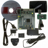
R0K561622S000BE
Manufacturer Part Number
R0K561622S000BE
Description
KIT STARTER FOR H8SX/1622
Manufacturer
Renesas Electronics America
Series
Renesas Starter Kits (RSK)r
Type
MCUr
Specifications of R0K561622S000BE
Contents
Board, Cables, CD, Debugger, Power Supply
Silicon Manufacturer
Renesas
Features
Coding And Debugging, E10A Emulator, RS232 Serial Connection
Kit Contents
Board
Silicon Family Name
H8SX/1622F
Silicon Core Number
R5F61622N50LGV
Lead Free Status / RoHS Status
Lead free / RoHS Compliant
For Use With/related Products
H8SX/1622
Lead Free Status / RoHS Status
Lead free / RoHS Compliant, Lead free / RoHS Compliant


Section 16 Serial Communication Interface (SCI)
16.6
Figure 16.14 shows the general format for clocked synchronous communication. In clocked
synchronous mode, data is transmitted or received in synchronization with clock pulses. One
character in transfer data consists of 8-bit data. In data transmission, the SCI outputs data from one
falling edge of the synchronization clock to the next. In data reception, the SCI receives data in
synchronization with the rising edge of the synchronization clock. After 8-bit data is output, the
transmission line holds the MSB output state. In clocked synchronous mode, no parity bit or
multiprocessor bit is added. Inside the SCI, the transmitter and receiver are independent units,
enabling full-duplex communication by use of a common clock. Both the transmitter and the
receiver also have a double-buffered structure, so that the next transmit data can be written during
transmission or the previous receive data can be read during reception, enabling continuous data
transfer.
16.6.1
Either an internal clock generated by the on-chip baud rate generator or an external
synchronization clock input at the SCK pin can be selected, according to the setting of the CKE1
and CKE0 bits in SCR. When the SCI is operated on an internal clock, the synchronization clock
is output from the SCK pin. Eight synchronization clock pulses are output in the transfer of one
character, and when no transfer is performed the clock is fixed high. Note that in the case of
reception only, the synchronization clock is output until an overrun error occurs or until the RE bit
is cleared to 0.
Rev. 2.00 Sep. 16, 2009 Page 654 of 1036
REJ09B0414-0200
Figure 16.14 Data Format in Clocked Synchronous Communication (LSB-First)
Operation in Clocked Synchronous Mode
Clock
Synchronization
clock
Serial data
Note: * Holds a high level except during continuous transfer.
Don't care
*
LSB
Bit 0
One unit of transfer data (character or frame)
Bit 1
Bit 2
Bit 3
Bit 4
Bit 5
Bit 6
MSB
Bit 7
Don't care
*
Related parts for R0K561622S000BE
Image
Part Number
Description
Manufacturer
Datasheet
Request
R

Part Number:
Description:
KIT STARTER FOR M16C/29
Manufacturer:
Renesas Electronics America
Datasheet:

Part Number:
Description:
KIT STARTER FOR R8C/2D
Manufacturer:
Renesas Electronics America
Datasheet:

Part Number:
Description:
R0K33062P STARTER KIT
Manufacturer:
Renesas Electronics America
Datasheet:

Part Number:
Description:
KIT STARTER FOR R8C/23 E8A
Manufacturer:
Renesas Electronics America
Datasheet:

Part Number:
Description:
KIT STARTER FOR R8C/25
Manufacturer:
Renesas Electronics America
Datasheet:

Part Number:
Description:
KIT STARTER H8S2456 SHARPE DSPLY
Manufacturer:
Renesas Electronics America
Datasheet:

Part Number:
Description:
KIT STARTER FOR R8C38C
Manufacturer:
Renesas Electronics America
Datasheet:

Part Number:
Description:
KIT STARTER FOR R8C35C
Manufacturer:
Renesas Electronics America
Datasheet:

Part Number:
Description:
KIT STARTER FOR R8CL3AC+LCD APPS
Manufacturer:
Renesas Electronics America
Datasheet:
Part Number:
Description:
KIT STARTER FOR RX610
Manufacturer:
Renesas Electronics America
Datasheet:

Part Number:
Description:
KIT STARTER FOR R32C/118
Manufacturer:
Renesas Electronics America
Datasheet:

Part Number:
Description:
KIT DEV RSK-R8C/26-29
Manufacturer:
Renesas Electronics America
Datasheet:

Part Number:
Description:
KIT STARTER FOR SH7124
Manufacturer:
Renesas Electronics America
Datasheet:

Part Number:
Description:
KIT DEV FOR SH7203
Manufacturer:
Renesas Electronics America
Datasheet:
Part Number:
Description:
KIT STARTER FOR R8C/18191A1B
Manufacturer:
Renesas Electronics America
Datasheet: