R0K561622S000BE Renesas Electronics America, R0K561622S000BE Datasheet - Page 744
R0K561622S000BE
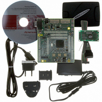
Manufacturer Part Number
R0K561622S000BE
Description
KIT STARTER FOR H8SX/1622
Manufacturer
Renesas Electronics America
Series
Renesas Starter Kits (RSK)r
Type
MCUr
Specifications of R0K561622S000BE
Contents
Board, Cables, CD, Debugger, Power Supply
Silicon Manufacturer
Renesas
Features
Coding And Debugging, E10A Emulator, RS232 Serial Connection
Kit Contents
Board
Silicon Family Name
H8SX/1622F
Silicon Core Number
R5F61622N50LGV
Lead Free Status / RoHS Status
Lead free / RoHS Compliant
For Use With/related Products
H8SX/1622
Lead Free Status / RoHS Status
Lead free / RoHS Compliant, Lead free / RoHS Compliant


Section 17 I
17.7.3
The WAIT bit in the I
when a slave device holds the SCL signal low more than one transfer clock cycle during the eighth
clock, the high level period of the ninth clock may be shorter than a given period.
17.7.4
When the I
be output with an unexpected pulse width. To avoid this phenomenon, set the I
this LSI to a value that is equal to or higher than 1/1.8 times the transfer rate of the fastest master.
For example, if the fastest rate of other master is 400 kbps, the I
be at least 223 kbps (= 400/1.8).
17.7.5
If the MST and TRS bits are manipulated sequentially to select master transmit mode, a conflict
state (for example, the AL bit in ICSR is set to 1 in master transmit mode (MST = 1, TRS = 1))
can result depending on the timing of arbitration lost that might occur during execution of the bit
manipulation instruction for the TRS bit. This phenomenon can be avoided by the following
operations.
• In multi-master mode, use the MOV instruction to set the MST and TRS bits.
• If arbitration is lost, check to see whether both MST and TRS bits have been cleared to 0. If
17.7.6
In master receive mode, when the value of RDRF is 1 at the falling edge of the eighth clock pulse,
the SCL signal is pulled low. If ICDRR is read near the falling edge of the eighth clock pulse, SCL
is fixed to low only during the eighth clock cycle of the next received data and, after that, SCL is
released even if ICDRR is not read, which allows the ninth clock pulse to be output. As a result,
some data fails to be received. This phenomenon can be avoided by the following operations.
• In master receive mode, read ICDRR before the rising edge of the eighth clock pulse.
• In master receive mode, set the RCVD bit to 1 and perform byte-wise communication.
Rev. 2.00 Sep. 16, 2009 Page 714 of 1036
REJ09B0414-0200
both bits are not clear, clear them to 0.
WAIT Bit
Restriction on Transfer Rate Setting Value in Multi-Master Mode
Restriction on Bit Manipulation when Setting the MST and TRS Bits in Multi-
Master Mode
Notes on Master Receive Mode
2
2
C transfer rate of this LSI is slower than that of any other master, the SCL signal may
C Bus Interface 2 (IIC2)
2
C bus mode register (ICMR) must be held 0. If the WAIT bit is set to 1,
2
C transfer rate of this LSI should
2
C transfer rate of
Related parts for R0K561622S000BE
Image
Part Number
Description
Manufacturer
Datasheet
Request
R

Part Number:
Description:
KIT STARTER FOR M16C/29
Manufacturer:
Renesas Electronics America
Datasheet:

Part Number:
Description:
KIT STARTER FOR R8C/2D
Manufacturer:
Renesas Electronics America
Datasheet:

Part Number:
Description:
R0K33062P STARTER KIT
Manufacturer:
Renesas Electronics America
Datasheet:

Part Number:
Description:
KIT STARTER FOR R8C/23 E8A
Manufacturer:
Renesas Electronics America
Datasheet:

Part Number:
Description:
KIT STARTER FOR R8C/25
Manufacturer:
Renesas Electronics America
Datasheet:

Part Number:
Description:
KIT STARTER H8S2456 SHARPE DSPLY
Manufacturer:
Renesas Electronics America
Datasheet:

Part Number:
Description:
KIT STARTER FOR R8C38C
Manufacturer:
Renesas Electronics America
Datasheet:

Part Number:
Description:
KIT STARTER FOR R8C35C
Manufacturer:
Renesas Electronics America
Datasheet:

Part Number:
Description:
KIT STARTER FOR R8CL3AC+LCD APPS
Manufacturer:
Renesas Electronics America
Datasheet:
Part Number:
Description:
KIT STARTER FOR RX610
Manufacturer:
Renesas Electronics America
Datasheet:

Part Number:
Description:
KIT STARTER FOR R32C/118
Manufacturer:
Renesas Electronics America
Datasheet:

Part Number:
Description:
KIT DEV RSK-R8C/26-29
Manufacturer:
Renesas Electronics America
Datasheet:

Part Number:
Description:
KIT STARTER FOR SH7124
Manufacturer:
Renesas Electronics America
Datasheet:

Part Number:
Description:
KIT DEV FOR SH7203
Manufacturer:
Renesas Electronics America
Datasheet:
Part Number:
Description:
KIT STARTER FOR R8C/18191A1B
Manufacturer:
Renesas Electronics America
Datasheet: