DK-DEV-2AGX260N Altera, DK-DEV-2AGX260N Datasheet - Page 31
DK-DEV-2AGX260N
Manufacturer Part Number
DK-DEV-2AGX260N
Description
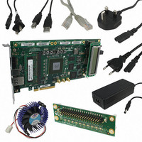
KIT DEV FPGA 2AGX260 W/6.375G TX
Manufacturer
Altera
Series
Arria II GXr
Type
FPGAr
Specifications of DK-DEV-2AGX260N
Contents
Board, Cables, CD, DVD, Power Supply
Silicon Manufacturer
Altera
Core Architecture
FPGA
Core Sub-architecture
Arria
Silicon Core Number
EP2
Silicon Family Name
Arria II GX
Rohs Compliant
Yes
For Use With/related Products
EP2AGX260
Lead Free Status / RoHS Status
Lead free / RoHS Compliant
Other names
544-2696
Available stocks
Company
Part Number
Manufacturer
Quantity
Price
Company:

Part Number:
DK-DEV-2AGX260N
Manufacturer:
Altera
Quantity:
135


Chapter 2: Board Components
General User Input/Output
Table 2–21. Crystal Oscillator Component References and Manufacturing Information
General User Input/Output
User-Defined Push-Button Switches
Table 2–22. User-defined Push-button Switch Schematic Signal Names and Functions
© July 2010 Altera Corporation
Board Reference
Reference
Board
U25
U26
U30
Y6
Y5
PB2
PB1
PB3
156.25 MHz LVPECL Saw
Oscillator
Quad Output Programmable
Clock Generator
Single Output Programmable
Clock Generator
100 MHz Crystal Oscillator
50 MHz Crystal Oscillator
User-defined push-button switch
Table 2–21
information.
This section describes the user I/O interface to the FPGA, including the push-buttons,
DIP switches, status LEDs, and character LCD.
The development board includes three user-defined push-button switches: two
general user push-button switches and one CPU reset. For information on the system
and safe reset push-button switches, refer to
Switches” on page
Board references PB1 and PB2 are push-button switches that allow you to interact
with the Arria II GX device. When the switch is pressed and held down, the device
pin is set to logic 0; when the switch is released, the device pin is set to logic 1. There is
no board-specific function for these general user push-button switches.
The board reference PB3 is the CPU reset push-button switch, CPU_RESET, which is
an input to the Arria II GX device. CPU_RESET is intended to be the master reset
signal for the FPGA design loaded into the Arria II GX device. It also acts as a regular
I/O pin.
Table 2–22
corresponding Arria II GX device pin numbers.
Description
Description
lists the user-defined push-button switch schematic signal names and their
lists the crystal oscillators component references and manufacturing
2–19.
Epson
Texas Instruments
Texas Instruments
Mercury Electronics 3H53-AT-100.000
Epson
Manufacturer
USER_PB0
USER_PB1
CPU_RESET
Schematic Signal
Name
Arria II GX FPGA Development Board, 6G Edition Reference Manual
CDCM61004RHBR
CDCM61001RHBR
EG-2102CA
155.5200M-DGPA
XG-1000CB
50.0000M-DCL3
Manufacturer
“Reset Configuration Push-button
Part Number
I/O Standard
1.8-V
2.5-V
www.eea.epson.com
www.ti.com
www.ti.com
www.mecxtal.com
www.eea.epson.com
Manufacturer Website
Arria II GX Device
Pin Number
AK9
AL7
N10
2–23
Related parts for DK-DEV-2AGX260N
Image
Part Number
Description
Manufacturer
Datasheet
Request
R

Part Number:
Description:
KIT DEV ARRIA II GX FPGA 2AGX125
Manufacturer:
Altera
Datasheet:

Part Number:
Description:
KIT DEV CYCLONE III LS EP3CLS200
Manufacturer:
Altera
Datasheet:

Part Number:
Description:
KIT DEV STRATIX IV FPGA 4SE530
Manufacturer:
Altera
Datasheet:

Part Number:
Description:
KIT DEV MAX V 5M570Z
Manufacturer:
Altera
Datasheet:

Part Number:
Description:
KIT DEV STRATIX V FPGA 5SGXEA7
Manufacturer:
Altera
Datasheet:

Part Number:
Description:
KIT DEVELOPMENT STRATIX III
Manufacturer:
Altera
Datasheet:

Part Number:
Description:
KIT DEVELOPMENT STRATIX IV
Manufacturer:
Altera
Datasheet:

Part Number:
Description:
KIT DEV ARRIA GX 1AGX60N
Manufacturer:
Altera
Datasheet:
Part Number:
Description:
KIT STARTER CYCLONE IV GX
Manufacturer:
Altera
Datasheet:
Part Number:
Description:
KIT DEVELOPMENT STRATIX IV
Manufacturer:
Altera
Datasheet:

Part Number:
Description:
CPLD, EP610 Family, ECMOS Process, 300 Gates, 16 Macro Cells, 16 Reg., 16 User I/Os, 5V Supply, 35 Speed Grade, 24DIP
Manufacturer:
Altera Corporation
Datasheet:
Part Number:
Description:
CPLD, EP610 Family, ECMOS Process, 300 Gates, 16 Macro Cells, 16 Reg., 16 User I/Os, 5V Supply, 15 Speed Grade, 24DIP
Manufacturer:
Altera Corporation
Datasheet: