ATAVRONEKIT Atmel, ATAVRONEKIT Datasheet - Page 41
ATAVRONEKIT
Manufacturer Part Number
ATAVRONEKIT
Description
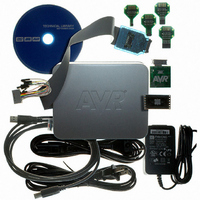
KIT AVR/AVR32 DEBUGGER/PROGRMMR
Manufacturer
Atmel
Series
AVR®r
Type
Debuggerr
Specifications of ATAVRONEKIT
Contents
Programmer/Debugger
Processor To Be Evaluated
AVR32
Data Bus Width
32 bit
Interface Type
ISP, JTAG
Core Architecture
AVR
Kit Contents
ATAVRONEKIT
Tool / Board Applications
General Purpose MCU, MPU, DSP, DSC
Development Tool Type
Hardware / Software - Dev Kit (Dev Tool)
Rohs Compliant
Yes
Mcu Supported Families
AVR32 32-bit MCU
For Use With/related Products
AVR® Devices
Lead Free Status / RoHS Status
Lead free / RoHS Compliant
Available stocks
Company
Part Number
Manufacturer
Quantity
Price
Company:

Part Number:
ATAVRONEKIT
Manufacturer:
Atmel
Quantity:
135


24. ADC - 12-bit Analog to Digital Converter
24.1
24.2
8067M–AVR–09/10
Features
Overview
•
•
•
•
•
•
•
•
•
•
•
•
•
XMEGA A1 devices have two Analog to Digital Converters (ADC), see
The two ADC modules can be operated simultaneously, individually or synchronized.
The ADC converts analog voltages to digital values. The ADC has 12-bit resolution and is capa-
ble of converting up to 2 million samples per second. The input selection is flexible, and both
single-ended and differential measurements can be done. For differential measurements an
optional gain stage is available to increase the dynamic range. In addition several internal signal
inputs are available. The ADC can provide both signed and unsigned results.
This is a pipeline ADC. A pipeline ADC consists of several consecutive stages, where each
stage convert one part of the result. The pipeline design enables high sample rate at low clock
speeds, and remove limitations on samples speed versus propagation delay. This also means
that a new analog voltage can be sampled and a new ADC measurement started while other
ADC measurements are ongoing.
ADC measurements can either be started by application software or an incoming event from
another peripheral in the device. Four different result registers with individual input selection
(MUX selection) are provided to make it easier for the application to keep track of the data. Each
result register and MUX selection pair is referred to as an ADC Channel. It is possible to use
DMA to move ADC results directly to memory or peripherals when conversions are done.
Both internal and external analog reference voltages can be used. An accurate internal 1.0V
reference is available.
An integrated temperature sensor is available and the output from this can be measured with the
ADC. The output from the DAC, VCC/10 and the Bandgap voltage can also be measured by the
ADC.
Two ADCs with 12-bit resolution
2 Msps sample rate for each ADC
Signed and Unsigned conversions
4 result registers with individual input channel control for each ADC
8 single ended inputs for each ADC
8x4 differential inputs for each ADC
4 internal inputs:
Software selectable gain of 2, 4, 8, 16, 32 or 64
Software selectable resolution of 8- or 12-bit.
Internal or External Reference selection
Event triggered conversion for accurate timing
DMA transfer of conversion results
Interrupt/Event on compare result
–
–
–
–
Integrated Temperature Sensor
DAC Output
VCC voltage divided by 10
Bandgap voltage
Figure 24-1 on page
XMEGA A1
42.
41
Related parts for ATAVRONEKIT
Image
Part Number
Description
Manufacturer
Datasheet
Request
R

Part Number:
Description:
DEV KIT FOR AVR/AVR32
Manufacturer:
Atmel
Datasheet:

Part Number:
Description:
INTERVAL AND WIPE/WASH WIPER CONTROL IC WITH DELAY
Manufacturer:
ATMEL Corporation
Datasheet:
Part Number:
Description:
Low-Voltage Voice-Switched IC for Hands-Free Operation
Manufacturer:
ATMEL Corporation
Datasheet:
Part Number:
Description:
MONOLITHIC INTEGRATED FEATUREPHONE CIRCUIT
Manufacturer:
ATMEL Corporation
Datasheet:
Part Number:
Description:
AM-FM Receiver IC U4255BM-M
Manufacturer:
ATMEL Corporation
Datasheet:
Part Number:
Description:
Monolithic Integrated Feature Phone Circuit
Manufacturer:
ATMEL Corporation
Datasheet:
Part Number:
Description:
Multistandard Video-IF and Quasi Parallel Sound Processing
Manufacturer:
ATMEL Corporation
Datasheet:
Part Number:
Description:
High-performance EE PLD
Manufacturer:
ATMEL Corporation
Datasheet:
Part Number:
Description:
8-bit Flash Microcontroller
Manufacturer:
ATMEL Corporation
Datasheet:
Part Number:
Description:
2-Wire Serial EEPROM
Manufacturer:
ATMEL Corporation
Datasheet: