MA300012 Microchip Technology, MA300012 Datasheet - Page 21
MA300012
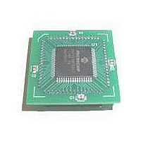
Manufacturer Part Number
MA300012
Description
MODULE DSPIC30F SAMPLE 64QFP
Manufacturer
Microchip Technology
Specifications of MA300012
Module/board Type
dsPIC30F Plug-in Module
Lead Free Status / RoHS Status
Lead free / RoHS Compliant
For Use With/related Products
DM240001
Lead Free Status / RoHS Status
Lead free / RoHS Compliant, Lead free / RoHS Compliant


7.0
System management services provided by the
dsPIC30F device family include:
• Control of clock options and oscillators
• Power-on Reset
• Programmable Brown-out Reset
• Program control of Power-up Timer
• Oscillator start-up timer/stabilizer
• Watchdog Timer with RC oscillator
• Fail-Safe Clock Monitor
• Reset by multiple sources
7.1
There are three primary clock oscillators: XTL, XT and
HS. The XTL oscillator is designed for crystals or
ceramic resonators in the range of 200 kHz to 4 MHz.
The XT oscillator is designed for crystals and ceramic
resonators in the range of 4 to 10 MHz. The HS (High-
Speed) oscillator is for crystals in the 10 to 25 MHz
range. These oscillators use the OSC1 and OSC2 pins.
The secondary (LP) oscillator is designed for low power
and uses a 32 kHz crystal or ceramic resonator. The LP
oscillator uses the SOSC1 and SOSC2 pins.
The FRC (Fast RC) internal oscillator runs at a nominal
7.37 MHz ±2%. The user software can tune the FRC
frequency. The LPRC (Low Power RC) internal
oscIllator is connected to the Watchdog Timer, and it
runs at a nominal 512 kHz. The External RC (ERC)
oscillator uses an external resistor and capacitor
connected to the OSC1 pin. Frequency of operation is
up to 4 MHz.
The OSC1 pin can also be used as an input from an
external clock source; this mode is called “EC”.
The dsPIC30F oscillator system provides:
• Various external and internal oscillator options as
• An on-chip PLL to boost internal operating
• In some devices, the FRC oscillator can also be
• Clock switching between various clock sources
• Programmable clock postscaler for system power
• A Fail-Safe Clock Monitor (FSCM) that detects
• A Clock Control register (OSCCON)
• Nonvolatile Configuration bits for main oscillator
A simplified block diagram of the oscillator system is
shown in Figure 7-1.
© 2005 Microchip Technology Inc.
clock sources
frequency 4, 8 or 16 times
used with the PLL
savings
clock failure and takes fail-safe measures
selection.
SYSTEM INTEGRATION
Clock Options and Oscillators
7.2
When a supply voltage is applied to the device, a
Power-on Reset is generated. A new Power-on Reset
event is generated if the supply voltage falls below the
device threshold voltage (V
pulse is generated when the rising supply voltage
crosses the POR circuit threshold voltage.
7.3
The BOR (Brown-out Reset) module is based on an
internal voltage reference circuit. The main purpose of
the BOR module is to generate a device Reset when a
brown-out condition occurs. Brown-out conditions are
generally caused by glitches on the AC mains (i.e.,
missing portions of the AC cycle waveform due to bad
power transmission lines or voltage sags due to
excessive current draw when a large inductive load is
turned on).
The BOR module allows selection of one of the
following voltage trip points:
• 2.0V
• 2.7V
• 4.2V
• 4.5V
A BOR generates a Reset pulse, which resets the
device.
Note:
Power-On Reset
Programmable Brown-out Reset
The BOR voltage trip points indicated here
are nominal values provided for design
guidance only. Refer to the Electrical
Specifications in the specific device data
sheet for BOR voltage limit specifications.
dsPIC30F
POR
). An internal POR
DS70043F-page 19
Related parts for MA300012
Image
Part Number
Description
Manufacturer
Datasheet
Request
R

Part Number:
Description:
Manufacturer:
Microchip Technology Inc.
Datasheet:
Part Number:
Description:
Manufacturer:
Microchip Technology Inc.
Datasheet:
Part Number:
Description:
Manufacturer:
Microchip Technology Inc.
Datasheet:
Part Number:
Description:
Manufacturer:
Microchip Technology Inc.
Datasheet:
Part Number:
Description:
Manufacturer:
Microchip Technology Inc.
Datasheet:
Part Number:
Description:
Manufacturer:
Microchip Technology Inc.
Datasheet:
Part Number:
Description:
Manufacturer:
Microchip Technology Inc.
Datasheet:
Part Number:
Description:
Manufacturer:
Microchip Technology Inc.
Datasheet: