EVAL-ADUC847QS Analog Devices Inc, EVAL-ADUC847QS Datasheet - Page 25
EVAL-ADUC847QS
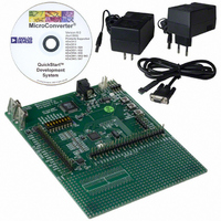
Manufacturer Part Number
EVAL-ADUC847QS
Description
KIT DEV FOR ADUC847 QUICK START
Manufacturer
Analog Devices Inc
Datasheet
1.EVAL-ADUC845QSZ.pdf
(108 pages)
Specifications of EVAL-ADUC847QS
Lead Free Status / RoHS Status
Lead free / RoHS Compliant


Power Control Register (PCON)
The PCON SFR contains bits for power-saving options and
general-purpose status flags as listed in Table 6.
SFR Address:
Power-On Default:
Bit Addressable:
Table 6. PCON SFR Bit Designations
Bit No.
7
6
5
4
3
2
1
0
Name
SMOD
SERIPD
INT0PD
ALEOFF
GF1
GF0
PD
-----
Description
Double UART Baud Rate.
0 = Normal, 1 = Double Baud Rate.
Serial Power-Down Interrupt Enable. If this
bit is set, a serial interrupt from either SPI
or I
mode.
INT0 Power-Down Interrupt Enable.
If this bit is set, either a level (IT0 = 0) or a
negative-going transition (IT0 = 1) on th
INT0 pin terminates power-down mode.
If set to 1, the ALE output is disabled.
General-Purpose Flag Bit.
General-Purpose Flag Bit.
Power-Down Mode Enable. If se
part enters power-down mode.
Not Implemented. Write Don’t Care.
87H
00H
No
2
C can terminate the power-down
t to 1, the
Rev. B | Page 25 of 108
e
ADuC845/ADuC847/ADuC848 Configuration Register
(CFG845/CFG847/CFG848)
The CFG845/CFG847/CFG848 SFR contains the bits necessary
to configure the internal XRAM and the extended SP. By default,
it configures the user into 8051 mode, that is, extended SP, and
the internal XRAM are disabled. When using in a program, use
the part name only, that is, CFG845, CFG847, or CFG8
SFR Address:
Power-On Default:
Bit Addressable:
Table 7. CFG845/CFG847/CFG848 SFR Bit Designations
Bit No.
7
6
5
4
3
2
1
0
Name
EXSP
----
----
----
----
----
----
XRAMEN
ADuC845/ADuC847/ADuC848
AFH
00H
No
Description
Extended SP Enable.
If this bit is set to 1, the stack rolls over
from SPH/SP = 00FFH to 0100H.
If this bit is cleared to 0, SPH SFR is
disabled and the stack rolls over from
SP = FFH to SP = 00H.
Not Implemented. Write Don’t Care.
Not Implemented. Write Don’t Care.
Not Implemented. Write Don’t Care.
Not Implemented. Write Don’t Care.
Not Implemented. Write Don’t Care.
Not Implemented. Write Don’t Care.
If this bit is set to 1, the internal XRAM is
mapped into the lower 2 kbytes of the
external address space.
If this bit is cleared to 0, the internal XR
is accessible and up to 16 MB of external
data memory become available. See
Figure 8.
48.
AM
Related parts for EVAL-ADUC847QS
Image
Part Number
Description
Manufacturer
Datasheet
Request
R


Part Number:
Description:
BOARD EVAL FOR SI270X-A
Manufacturer:
Silicon Laboratories Inc
Datasheet:

Part Number:
Description:
BUCK CONV REF DESIGN KIT IP1201
Manufacturer:
International Rectifier
Datasheet:
Part Number:
Description:
BOARD DEMO SYNC DUAL BUCK CNVTER
Manufacturer:
International Rectifier
Datasheet:
Part Number:
Description:
BOARD DEMO SYNC BUCK CONVETER
Manufacturer:
International Rectifier
Datasheet:

Part Number:
Description:
EVALBOARD/EB Omnidirectional microphone - Analog
Manufacturer:
Analog Devices
Datasheet:
Part Number:
Description:
EVALBOARD/EB Omnidirectional microphone - Analog
Manufacturer:
Analog Devices
Datasheet:


Part Number:
Description:
BOARD EVAL LED DRIVER LT3756
Manufacturer:
Linear Technology
Datasheet:

Part Number:
Description:
BOARD EVAL FOR AD7741/7742
Manufacturer:
Analog Devices Inc
Datasheet:

Part Number:
Description:
±1.7g Dual-Axis IMEMS Accelerometer Evaluation Board
Manufacturer:
Analog Devices Inc
Datasheet:

Part Number:
Description:
IC MULTIPLIER ANALOG 8-SOIC T/R
Manufacturer:
Analog Devices Inc
Datasheet:

Part Number:
Description:
IC ANALOG MULTIPLIER 8-DIP
Manufacturer:
Analog Devices Inc
Datasheet:
Part Number:
Description:
IC ANALOG MULTIPLIER 8-SOIC
Manufacturer:
Analog Devices Inc
Datasheet:
Part Number:
Description:
IC ANALOG MULTIPLIER 8-DIP
Manufacturer:
Analog Devices Inc
Datasheet: