AD9958/PCB Analog Devices Inc, AD9958/PCB Datasheet - Page 10
AD9958/PCB
Manufacturer Part Number
AD9958/PCB
Description
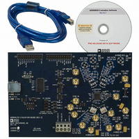
BOARD EVALUATION FOR AD9958
Manufacturer
Analog Devices Inc
Datasheet
1.AD9958BCPZ.pdf
(44 pages)
Specifications of AD9958/PCB
Design Resources
Low Jitter Sampling Clock Generator for High Performance ADCs Using AD9958/9858 and AD9515 (CN0109) Phase Coherent FSK Modulator (CN0186)
Lead Free Status / RoHS Status
Contains lead / RoHS non-compliant
Available stocks
Company
Part Number
Manufacturer
Quantity
Price
Company:

Part Number:
AD9958/PCBZ
Manufacturer:
Analog Devices Inc
Quantity:
135


AD9958
Pin No.
24
27
28, 32, 34, 38
40, 41, 42, 43
46
47
48
49
50
51, 52, 53
54
1
I = input, O = output.
Mnemonic
CLK_MODE_SEL
LOOP_FILTER
NC
P0, P1, P2, P3
I/O_UPDATE
CS
SCLK
DVDD_I/O
SDIO_0
SDIO_1, SDIO_2,
SDIO_3
SYNC_CLK
I/O
I
I
N/A
I
I
I
I
I
I/O
I/O
O
1
Active Low Chip Select. Allows multiple devices to share a common I/O bus (SPI).
3.3 V Digital Power Supply for SPI Port and Digital I/O.
Data Pin SDIO_0 is dedicated to the serial port I/O only.
Description
Control Pin for the Oscillator Section. Caution: Do not drive this pin beyond 1.8 V.
When high (1.8 V), the oscillator section is enabled to accept a crystal as the
REF_CLK source. When low, the oscillator section is bypassed.
Connects to the external zero compensation network of the PLL loop filter.
Typically, the network consists of a 0 Ω resistor in series with a 680 pF capacitor
tied to AVDD.
No Connection.
Data pins used for modulation (FSK, PSK, ASK), to start/stop for the sweep
accumulators, or used to ramp up/ramp down the output amplitude. The data is
synchronous to the SYNC_CLK (Pin 54). The data inputs must meet the setup and
hold time requirements to the SYNC_CLK. The functionality of these pins is
controlled by profile pin configuration (PPC) bits (FR1[14:12]).
A rising edge transfers data from the serial I/O port buffer to active registers.
I/O_UPDATE is synchronous to the SYNC_CLK (Pin 54). I/O_UPDATE must meet the
setup and hold time requirements to the SYNC_CLK to guarantee a fixed pipeline
delay of data to the DAC output; otherwise, a ±1 SYNC_CLK period of pipeline
uncertainty exists. The minimum pulse width is one SYNC_CLK period.
Serial Data Clock for I/O Operations. Data bits are written on the rising edge of
SCLK and read on the falling edge of SCLK.
Data Pin SDIO_1, Data Pin SDIO_2, and Data Pin SDIO_3 can be used for the serial
I/O port or used to initiate a ramp-up/ramp-down (RU/RD) of the DAC output
amplitude.
The SYNC_CLK runs at one fourth the system clock rate. It can be disabled. I/O_UPDATE
or data (Pin 40 to Pin 43) is synchronous to the SYNC_CLK. To guarantee a fixed
pipeline delay of data to DAC output, I/O_UPDATE or data (Pin 40 to Pin 43) must
meet the setup and hold time requirements to the rising edge of SYNC_CLK;
otherwise, a ±1 SYNC_CLK period of uncertainty exists.
Rev. A | Page 10 of 44
Related parts for AD9958/PCB
Image
Part Number
Description
Manufacturer
Datasheet
Request
R

Part Number:
Description:
BOARD EVALUATION FOR AD9958
Manufacturer:
Analog Devices Inc
Datasheet:


Part Number:
Description:
±1.7g Dual-Axis IMEMS Accelerometer Evaluation Board
Manufacturer:
Analog Devices Inc
Datasheet:

Part Number:
Description:
Inertial Sensor Evaluation System
Manufacturer:
Analog Devices Inc
Datasheet:
Part Number:
Description:
Manufacturer:
Analog Devices Inc
Datasheet:
Part Number:
Description:
Manufacturer:
Analog Devices Inc
Datasheet:
Part Number:
Description:
Manufacturer:
Analog Devices Inc
Datasheet:
Part Number:
Description:
Manufacturer:
Analog Devices Inc
Datasheet:
Part Number:
Description:
Manufacturer:
Analog Devices Inc
Datasheet:
Part Number:
Description:
Manufacturer:
Analog Devices Inc
Datasheet:
Part Number:
Description:
Manufacturer:
Analog Devices Inc
Datasheet:
Part Number:
Description:
Manufacturer:
Analog Devices Inc
Datasheet:
Part Number:
Description:
Manufacturer:
Analog Devices Inc
Datasheet: