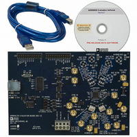
AD9958/PCB Analog Devices Inc, AD9958/PCB Datasheet - Page 18

AD9958/PCB
Manufacturer Part Number
AD9958/PCB
Description
BOARD EVALUATION FOR AD9958
Manufacturer
Analog Devices Inc
Datasheet
1.AD9958BCPZ.pdf
(44 pages)
Specifications of AD9958/PCB
Design Resources
Low Jitter Sampling Clock Generator for High Performance ADCs Using AD9958/9858 and AD9515 (CN0109) Phase Coherent FSK Modulator (CN0186)
Lead Free Status / RoHS Status
Contains lead / RoHS non-compliant
Available stocks
Company
Part Number
Manufacturer
Quantity
Price
Company:
Part Number:
AD9958/PCBZ
Manufacturer:
Analog Devices Inc
Quantity:
135
AD9958
THEORY OF OPERATION
DDS CORE
The AD9958 has two DDS cores, each consisting of a 32-bit
phase accumulator and phase-to-amplitude converter. Together,
these digital blocks generate a digital sine wave when the phase
accumulator is clocked and the phase increment value (frequency
tuning word) is greater than 0. The phase-to-amplitude converter
simultaneously translates phase information to amplitude
information by a cos(θ) operation.
The output frequency (f
of the rollover rate of each phase accumulator. The exact
relationship is given in the following equation:
where:
f
FTW is the frequency tuning word and is 0 ≤ FTW ≤ 2
2
Because both channels share a common system clock, they are
inherently synchronized.
The DDS core architecture also supports the capability to phase
offset the output signal, which is performed by the channel
phase offset word (CPOW). The CPOW is a 14-bit register that
stores a phase offset value. This value is added to the output of
the phase accumulator to offset the current phase of the output
signal. Each channel has its own phase offset word register. This
feature can be used for placing all channels in a known phase
relationship relative to one another. The exact value of phase
offset is given by the following equation:
S
32
is the system clock rate.
represents the phase accumulator capacity.
Φ
f
OUT
=
⎛
⎜
⎝
=
POW
(
2
FTW
14
2
32
⎞
⎟
⎠
)(
×
f
360
S
)
OUT
°
) of each DDS channel is a function
31
.
Rev. A | Page 18 of 44
DIGITAL-TO-ANALOG CONVERTER
The AD9958 incorporates four 10-bit current output DACs.
The DAC converts a digital code (amplitude) into a discrete
analog quantity. The DAC current outputs can be modeled as a
current source with high output impedance (typically 100 kΩ).
Unlike many DACs, these current outputs require termination
into AVDD via a resistor or a center-tapped transformer for
expected current flow.
Each DAC has complementary outputs that provide a combined
full-scale output current (I
current, and their sum equals the full-scale current at any point
in time. The full-scale current is controlled by means of an
external resistor (R
bits discussed in the Modes of Operation section. The resistor,
R
ground (AGND). The full-scale current is inversely proportional
to the resistor value as follows:
The maximum full-scale output current of the combined DAC
outputs is 15 mA, but limiting the output to 10 mA provides
optimal spurious-free dynamic range (SFDR) performance.
The DAC output voltage compliance range is AVDD + 0.5 V to
AVDD − 0.5 V. Voltages developed beyond this range may cause
excessive harmonic distortion. Proper attention should be paid
to the load termination to keep the output voltage within its
compliance range. Exceeding this range could potentially dam-
age the DAC output circuitry.
SET
, is connected between the DAC_RSET pin and analog
R
SET
Figure 32. Typical DAC Output Termination Configuration
=
DAC
I
OUT
18
.
(max)
91
SET
CHx_IOUT
CHx_IOUT
) and the scalable DAC current control
AVDD
OUT
+ I
1:1
OUT
). The outputs always sink
LPF
50Ω


