AD9958/PCB Analog Devices Inc, AD9958/PCB Datasheet - Page 19
AD9958/PCB
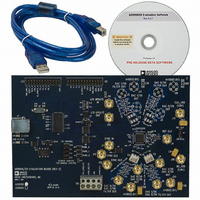
Manufacturer Part Number
AD9958/PCB
Description
BOARD EVALUATION FOR AD9958
Manufacturer
Analog Devices Inc
Datasheet
1.AD9958BCPZ.pdf
(44 pages)
Specifications of AD9958/PCB
Design Resources
Low Jitter Sampling Clock Generator for High Performance ADCs Using AD9958/9858 and AD9515 (CN0109) Phase Coherent FSK Modulator (CN0186)
Lead Free Status / RoHS Status
Contains lead / RoHS non-compliant
Available stocks
Company
Part Number
Manufacturer
Quantity
Price
Company:

Part Number:
AD9958/PCBZ
Manufacturer:
Analog Devices Inc
Quantity:
135


MODES OF OPERATION
There are many combinations of modes (for example, single-
tone, modulation, linear sweep) that the AD9958 can perform
simultaneously. However, some modes require multiple data
pins, which can impose limitations. The following guidelines
can help determine if a specific combination of modes can be
performed simultaneously by the AD9958.
CHANNEL CONSTRAINT GUIDELINES
•
•
•
•
•
•
•
•
•
•
•
Single-tone mode, two-level modulation mode, and linear
sweep mode can be enabled on either channel and in any
combination simultaneously.
Both channels can perform four-level modulation
simultaneously.
Either channel can perform eight-level or 16-level
modulation. The other channel can only be in single-tone
mode.
The RU/RD function can be used on both channels in
single-tone mode. See the Output Amplitude Control
Mode section for the RU/RD function.
When Profile Pin P2 and Profile Pin P3 are used for
RU/RD, either channel can perform two-level modulation
with RU/RD or both channels can perform linear
frequency or phase sweep with RU/RD.
When Profile Pin P3 is used for RU/RD, either channel can
be used in eight-level modulation with RU/RD. The other
channel can only be in single-tone mode.
When SDIO_1, SDIO_2, and SDIO_3 pins are used for
RU/RD, either or both channels can perform two-level
modulation with RU/RD. If one channel is not in two-level
modulation, it can only be in single-tone mode.
When the SDIO_1, SDIO_2, and SDIO_3 pins are used for
RU/RD, either or both channels can perform four-level
modulation with RU/RD. If one channel is not in four-level
modulation, it can only be in single-tone mode.
When the SDIO_1, SDIO_2, and SDIO_3 pins are used for
RU/RD, either channel can perform eight-level modulation
with RU/RD. The other channel can only be in single-tone
mode.
When the SDIO_1, SDIO_2, and SDIO_3 pins are used for
RU/RD, either channel can perform 16-level modulation with
RU/RD. The other channel can only be in single-tone mode.
Amplitude modulation, linear amplitude sweep modes,
and the RU/RD function cannot operate simultaneously,
but frequency and phase modulation can operate
simultaneously with the RU/RD function.
Rev. A | Page 19 of 44
POWER SUPPLIES
The AVDD and DVDD supply pins provide power to the DDS
core and supporting analog circuitry. These pins connect to a
1.8 V nominal power supply.
The DVDD_I/O pin connects to a 3.3 V nominal power supply.
All digital inputs are 3.3 V logic except for the CLK_MODE_SEL
input. CLK_MODE_SEL (Pin 24) is an analog input and should
be operated by 1.8 V logic.
SINGLE-TONE MODE
Single-tone mode is the default mode of operation after a master
reset signal. In this mode, both DDS channels share a common
address location for the frequency tuning word (Register 0x04)
and phase offset word (Register 0x05). Channel enable bits are
provided in combination with these shared addresses. As a
result, the frequency tuning word and/or phase offset word can
be independently programmed between channels (see the follow-
ing Step 1 through Step 5). The channel enable bits do not
require an I/O update to enable or disable a channel.
See the Register Maps and Bit Descriptions section for a
description of the channel enable bits in the channel select
register (CSR, Register 0x00). The channel enable bits are
enabled or disabled immediately after the CSR data byte is
written.
Address sharing enables channels to be written simultaneously,
if desired. The default state enables all channel enable bits.
Therefore, the frequency tuning word and/or phase offset word
is common to all channels but written only once through the
serial I/O port.
The following steps present a basic protocol to program a
different frequency tuning word and/or phase offset word for
each channel using the channel enable bits.
1.
2.
3.
4.
5.
Power up the DUT and issue a master reset. A master reset
places the part in single-tone mode and single-bit mode for
serial programming operations (refer to the Serial I/O Modes
of Operation section). Frequency tuning words and phase
offset words default to 0 at this point.
Enable only one channel enable bit (Register 0x00) and
disable the other channel enable bit.
Using the serial I/O port, program the desired frequency
tuning word (Register 0x04) and/or the phase offset word
(Register 0x05) for the enabled channel.
Repeat Step 2 and Step 3 for each channel.
Send an I/O update signal. After an I/O update, all
channels should output their programmed frequency
and/or phase offset values.
AD9958
Related parts for AD9958/PCB
Image
Part Number
Description
Manufacturer
Datasheet
Request
R

Part Number:
Description:
BOARD EVALUATION FOR AD9958
Manufacturer:
Analog Devices Inc
Datasheet:


Part Number:
Description:
±1.7g Dual-Axis IMEMS Accelerometer Evaluation Board
Manufacturer:
Analog Devices Inc
Datasheet:

Part Number:
Description:
Inertial Sensor Evaluation System
Manufacturer:
Analog Devices Inc
Datasheet:
Part Number:
Description:
Manufacturer:
Analog Devices Inc
Datasheet:
Part Number:
Description:
Manufacturer:
Analog Devices Inc
Datasheet:
Part Number:
Description:
Manufacturer:
Analog Devices Inc
Datasheet:
Part Number:
Description:
Manufacturer:
Analog Devices Inc
Datasheet:
Part Number:
Description:
Manufacturer:
Analog Devices Inc
Datasheet:
Part Number:
Description:
Manufacturer:
Analog Devices Inc
Datasheet:
Part Number:
Description:
Manufacturer:
Analog Devices Inc
Datasheet:
Part Number:
Description:
Manufacturer:
Analog Devices Inc
Datasheet:
Part Number:
Description:
Manufacturer:
Analog Devices Inc
Datasheet: