AD9958/PCB Analog Devices Inc, AD9958/PCB Datasheet - Page 25
AD9958/PCB
Manufacturer Part Number
AD9958/PCB
Description
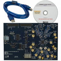
BOARD EVALUATION FOR AD9958
Manufacturer
Analog Devices Inc
Datasheet
1.AD9958BCPZ.pdf
(44 pages)
Specifications of AD9958/PCB
Design Resources
Low Jitter Sampling Clock Generator for High Performance ADCs Using AD9958/9858 and AD9515 (CN0109) Phase Coherent FSK Modulator (CN0186)
Lead Free Status / RoHS Status
Contains lead / RoHS non-compliant
Available stocks
Company
Part Number
Manufacturer
Quantity
Price
Company:

Part Number:
AD9958/PCBZ
Manufacturer:
Analog Devices Inc
Quantity:
135


LINEAR SWEEP MODE
Linear sweep mode enables the user to sweep frequency, phase,
or amplitude from a starting point (S0) to an endpoint (E0).
The purpose of linear sweep mode is to provide better band-
width containment compared to direct modulation by replacing
greater instantaneous changes with more gradual, user-defined
changes between S0 and E0.
In linear sweep mode, S0 is loaded into the Channel Word 0
register (S0 is represented by one of three registers: Register 0x04,
Register 0x05, or Register 0x06, depending on the type of sweep)
and E0 is always loaded into Channel Word 1 (Register 0x0A).
If E0 is configured for frequency sweep, the resolution is 32 bits,
phase sweep is 14 bits, and amplitude sweep is 10 bits. When
sweeping phase or amplitude, the word value must be MSB aligned
in the Channel Word 1 register. The unused bits are don’t care
bits. The profile pins are used to trigger and control the direction
of the linear sweep for frequency, phase, and amplitude. All
channels can be programmed separately for a linear sweep. In
linear sweep mode, Profile Pin P0 is dedicated to Channel 0.
Profile Pin P1 is dedicated to Channel 1, and so on.
The AD9958 has the ability to ramp up or ramp down (RU/RD)
the output amplitude (using the 10-bit output scalar) before and
after a linear sweep. If the RU/RD feature is desired, unused
profile pins or unused SDIO_1/SDIO_2/SDIO_3 pins can be
configured for the RU/RD operation.
To enable linear sweep mode for a particular channel, the AFP
select bits (CFR[23:22]), the modulation level bits (FR1[9:8]),
and the linear sweep enable bit (CFR[14]) are programmed.
The AFP select bits determine the type of linear sweep to be
performed. The modulation level bits must be set to 00 (two-
level) for that specific channel (see Table 19 and Table 20)
Table 19. Linear Sweep Parameter to Sweep
AFP Select
(CFR[23:22])
00
01
10
11
Table 20. Modulation Level Assignments
Modulation Level (FR1[9:8])
00 (Required in Linear Sweep)
01
10
11
Linear Sweep Enable
(CFR[14])
1
1
1
1
Description
Two-level modulation
Four-level modulation
Eight-level modulation
16-level modulation
Description
N/A
Amplitude sweep
Frequency sweep
Phase sweep
Rev. A | Page 25 of 44
Setting the Slope of the Linear Sweep
The slope of the linear sweep is set by the intermediate step size
(delta-tuning word) between S0 and E0 and the time spent
(sweep ramp rate word) at each step. The resolution of the
delta-tuning word is 32 bits for frequency, 14 bits for phase, and
10 bits for amplitude. The resolution for the delta ramp rate
word is eight bits.
In linear sweep, each channel is assigned a rising delta word
(RDW, Register 0x08) and a rising sweep ramp rate word
(RSRR, Register 0x07). These settings apply when sweeping up
toward E0. The falling delta word (FDW, Register 0x09) and
falling sweep ramp rate (FSRR, Register 0x07) apply when
sweeping down toward S0. Figure 36 displays a linear sweep up
and then down using a profile pin. Note that the linear sweep
no-dwell bit is disabled; otherwise, the sweep accumulator
returns to 0 upon reaching E0.
For a piecemeal or a nonlinear transition between S0 and E0,
the delta-tuning words and ramp rate words can be repro-
grammed during the transition to produce the desired response.
The formulas for calculating the step size of RDW or FDW for
delta frequency, delta phase, or delta amplitude are as follows:
The formula for calculating delta time from RSRR or FSRR is
At 500 MSPS operation (SYNC_CLK = 125 MHz), the maxi-
mum time interval between steps is 1/125 MHz × 256 = 2.048 μs.
The minimum time interval is (1/125 MHz) × 1 = 8.0 ns.
The sweep ramp rate block (timer) consists of a loadable 8-bit
down counter that continuously counts down from the loaded
value to 1. When the ramp rate timer equals 1, the proper ramp rate
value is loaded and the counter begins counting down to 1 again.
E0
S0
t
Δ
ΔΦ
Δ
=
f
a
=
(
=
=
RSRR
⎛
⎜
⎝
⎛
⎜
⎝
⎛
⎜
⎝
RDW
RDW
Δf,p,a
RDW
2
2
2
32
10
)
14
RDW
PROFILE PIN
×
Figure 36. Linear Sweep Parameters
/ 1
⎞
⎟
⎠
⎞
⎟
⎠
×
⎞
⎟
⎠
SYNC
×
×
SYSCLK
1024
Δt
360
°
_
CLK
(DAC full-scale current)
RSRR
(Hz)
TIME
FSRR
Δt
FDW
AD9958
Δf,p,a
Related parts for AD9958/PCB
Image
Part Number
Description
Manufacturer
Datasheet
Request
R

Part Number:
Description:
BOARD EVALUATION FOR AD9958
Manufacturer:
Analog Devices Inc
Datasheet:


Part Number:
Description:
±1.7g Dual-Axis IMEMS Accelerometer Evaluation Board
Manufacturer:
Analog Devices Inc
Datasheet:

Part Number:
Description:
Inertial Sensor Evaluation System
Manufacturer:
Analog Devices Inc
Datasheet:
Part Number:
Description:
Manufacturer:
Analog Devices Inc
Datasheet:
Part Number:
Description:
Manufacturer:
Analog Devices Inc
Datasheet:
Part Number:
Description:
Manufacturer:
Analog Devices Inc
Datasheet:
Part Number:
Description:
Manufacturer:
Analog Devices Inc
Datasheet:
Part Number:
Description:
Manufacturer:
Analog Devices Inc
Datasheet:
Part Number:
Description:
Manufacturer:
Analog Devices Inc
Datasheet:
Part Number:
Description:
Manufacturer:
Analog Devices Inc
Datasheet:
Part Number:
Description:
Manufacturer:
Analog Devices Inc
Datasheet:
Part Number:
Description:
Manufacturer:
Analog Devices Inc
Datasheet: