AD9958/PCB Analog Devices Inc, AD9958/PCB Datasheet - Page 29
AD9958/PCB
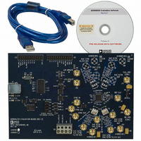
Manufacturer Part Number
AD9958/PCB
Description
BOARD EVALUATION FOR AD9958
Manufacturer
Analog Devices Inc
Datasheet
1.AD9958BCPZ.pdf
(44 pages)
Specifications of AD9958/PCB
Design Resources
Low Jitter Sampling Clock Generator for High Performance ADCs Using AD9958/9858 and AD9515 (CN0109) Phase Coherent FSK Modulator (CN0186)
Lead Free Status / RoHS Status
Contains lead / RoHS non-compliant
Available stocks
Company
Part Number
Manufacturer
Quantity
Price
Company:

Part Number:
AD9958/PCBZ
Manufacturer:
Analog Devices Inc
Quantity:
135


SYNCHRONIZING MULTIPLE AD9958 DEVICES
The AD9958 allows easy synchronization of multiple AD9958
devices. At power-up, the phase of SYNC_CLK can be offset
between multiple devices. To correct for the offset and align the
SYNC_CLK edges, there are three methods (one automatic mode
and two manual modes) of synchronizing the SYNC_CLK edges.
These modes force the internal state machines of multiple
devices to a known state, which aligns the SYNC_CLK edges.
In addition, the user must send a coincident I/O_UPDATE to
multiple devices to maintain synchronization. Any mismatch in
REF_CLK phase between devices results in a corresponding
phase mismatch on the SYNC_CLK edges.
AUTOMATIC MODE SYNCHRONIZATION
In automatic mode, multiple part synchronization is achieved
by connecting the SYNC_OUT pin on the master device to the
SYNC_IN pins of the slave devices. Devices are configured as
master or slave through programming bits, accessible via the
serial port.
A configuration for synchronizing multiple AD9958 devices in
automatic mode is shown in the Application Circuits section. In
this configuration, the AD9510 provides coincident REF_CLK
and SYNC_OUT signals to all devices.
Operation
The first step is to program the master and slave devices for
their respective roles and then write the auto sync enable bit
(FR2[7] = 1. Enabling the master device is performed by writing
its multidevice sync master enable bit in Function Register 2
(FR2[6]) = 1. This causes the SYNC_OUT of the master device
to output a pulse that has a pulse width equal to one system
clock period and a frequency equal to one-fourth of the system
clock frequency. Enabling devices as slaves is performed by
writing FR2[6] = 0.
In automatic synchronizing mode, the slave devices sample
SYNC_OUT pulses from the master device on the SYNC_IN
of the slave devices, and a comparison of all state machines is
made by the autosynchronization circuitry. If the slave devices
state machines are not identical to the master, the slave devices
state machines are stalled for one system clock cycle. This proce-
dure synchronizes the slave devices within three SYNC_CLK
periods.
Delay Time Between SYNC_OUT and SYNC_IN
When the delay between SYNC_OUT and SYNC_IN exceeds
one system clock period, the system clock offset bits (FR2[1:0])
are used to compensate. The default state of these bits is 00, which
implies that the SYNC_OUT of the master and the SYNC_IN of
the slave have a propagation delay of less than one system clock
period. If the propagation time is greater than one system clock
period, the time should be measured and the appropriate offset
programmed. Table 24 describes the delays required per system
clock offset value.
Rev. A | Page 29 of 44
Table 24. System Clock Offset (Delay) Assignments
System Clock
Offset (FR2[1:0])
00
01
10
11
Automatic Synchronization Status Bits
If a slave device falls out of sync, the sync status bit is set high.
The multidevice sync status bit (FR2[5]) can be read through
the serial port. It is automatically cleared when read.
The synchronization routine continues to operate regardless of
the state of FR2[5]. FR2[5] can be masked by writing Logic 1 to
the multidevice sync mask bit (FR2[4]). If FR2[5] is masked, it is
held low.
MANUAL SOFTWARE MODE SYNCHRONIZATION
Manual software mode is enabled by setting the manual software
sync bit (FR1[0]) to Logic 1 in a device. In this mode, the I/O
update that writes the manual software sync bit to Logic 0 stalls
the state machine of the clock generator for one system clock
cycle. Stalling the clock generation state machine by one cycle
changes the phase relationship of SYNC_CLK between devices
by one system clock period (90°).
Note that the user may have to repeat this process until the
devices have their SYNC_CLK signals in phase. The SYNC_IN
input can be left floating because it has an internal pull-up. The
SYNC_OUT pin is not used.
The synchronization is complete when the master and slave
devices have their SYNC_CLK signals in phase.
MANUAL HARDWARE MODE SYNCHRONIZATION
Manual hardware mode is enabled by setting the manual hardware
sync bit (FR1[1]) to Logic 1 in a device. In manual hardware
synchronization mode, the SYNC_CLK stalls by one system
clock cycle each time a rising edge is detected on the SYNC_IN
input. Stalling the SYNC_CLK state machine by one cycle changes
the phase relationship of SYNC_CLK between devices by one
system clock period (90°).
Note that the user may have to repeat the process until the devices
have their SYNC_CLK signals in phase. The SYNC_IN input
can be left floating because it has an internal pull-up. The
SYNC_OUT is not used.
The synchronization is complete when the master and slave
devices have their SYNC_CLK signals in phase.
SYNC_OUT/SYNC_IN
Propagation Delay
0 ≤ delay ≤ 1
1 ≤ delay ≤ 2
2 ≤ delay ≤ 3
3 ≤ delay ≤ 4
AD9958
Related parts for AD9958/PCB
Image
Part Number
Description
Manufacturer
Datasheet
Request
R

Part Number:
Description:
BOARD EVALUATION FOR AD9958
Manufacturer:
Analog Devices Inc
Datasheet:


Part Number:
Description:
±1.7g Dual-Axis IMEMS Accelerometer Evaluation Board
Manufacturer:
Analog Devices Inc
Datasheet:

Part Number:
Description:
Inertial Sensor Evaluation System
Manufacturer:
Analog Devices Inc
Datasheet:
Part Number:
Description:
Manufacturer:
Analog Devices Inc
Datasheet:
Part Number:
Description:
Manufacturer:
Analog Devices Inc
Datasheet:
Part Number:
Description:
Manufacturer:
Analog Devices Inc
Datasheet:
Part Number:
Description:
Manufacturer:
Analog Devices Inc
Datasheet:
Part Number:
Description:
Manufacturer:
Analog Devices Inc
Datasheet:
Part Number:
Description:
Manufacturer:
Analog Devices Inc
Datasheet:
Part Number:
Description:
Manufacturer:
Analog Devices Inc
Datasheet:
Part Number:
Description:
Manufacturer:
Analog Devices Inc
Datasheet:
Part Number:
Description:
Manufacturer:
Analog Devices Inc
Datasheet: