AD9958/PCB Analog Devices Inc, AD9958/PCB Datasheet - Page 3
AD9958/PCB
Manufacturer Part Number
AD9958/PCB
Description
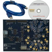
BOARD EVALUATION FOR AD9958
Manufacturer
Analog Devices Inc
Datasheet
1.AD9958BCPZ.pdf
(44 pages)
Specifications of AD9958/PCB
Design Resources
Low Jitter Sampling Clock Generator for High Performance ADCs Using AD9958/9858 and AD9515 (CN0109) Phase Coherent FSK Modulator (CN0186)
Lead Free Status / RoHS Status
Contains lead / RoHS non-compliant
Available stocks
Company
Part Number
Manufacturer
Quantity
Price
Company:

Part Number:
AD9958/PCBZ
Manufacturer:
Analog Devices Inc
Quantity:
135


GENERAL DESCRIPTION
The AD9958 consists of two DDS cores that provide indepen-
dent frequency, phase, and amplitude control on each channel.
This flexibility can be used to correct imbalances between
signals due to analog processing, such as filtering, amplification,
or PCB layout related mismatches. Because both channels share
a common system clock, they are inherently synchronized.
Synchronization of multiple devices is supported.
The AD9958 can perform up to a 16-level modulation of
frequency, phase, or amplitude (FSK, PSK, ASK). Modulation is
performed by applying data to the profile pins. In addition, the
AD9958 also supports linear sweep of frequency, phase, or
amplitude for applications such as radar and instrumentation.
The AD9958 serial I/O port offers multiple configurations to
provide significant flexibility. The serial I/O port offers an SPI-
compatible mode of operation that is virtually identical to the
SPI operation found in earlier Analog Devices, Inc., DDS
products. Flexibility is provided by four data pins (SDIO_0/
SDIO_1/SDIO_2/SDIO_3) that allow four programmable
modes of serial I/O operation.
The AD9958 uses advanced DDS technology that provides low
power dissipation with high performance. The device incorporates
two integrated, high speed 10-bit DACs with excellent wideband
and narrow-band SFDR. Each channel has a dedicated 32-bit
frequency tuning word, 14 bits of phase offset, and a 10-bit
output scale multiplier.
I/O_UPDATE
SYNC_OUT
SYNC_CLK
REF_CLK
REF_CLK
SYNC_IN
AD9958
CLK_MODE_SEL
ΔFTW
OSCILLATOR
BUFFER/
XTAL
÷4
32
32
FTW
MULTIPLIER
REF CLOCK
4× TO 20×
Σ
Σ
32
32
32
Figure 2. Detailed Block Diagram
Σ
Σ
TIMING AND CONTROL LOGIC
PHASE/
ΔPHASE
SYSTEM
CLK
MUX
Rev. A | Page 3 of 44
Σ
Σ
AVDD
1.8V
14
15
15
DDS CORE
DVDD
COS(X)
COS(X)
1.8V
The DAC outputs are supply referenced and must be termin-
ated into AVDD by a resistor or an AVDD center-tapped
transformer. Each DAC has its own programmable reference to
enable different full-scale currents for each channel.
The DDS acts as a high resolution frequency divider with the
REFCLK as the input and the DAC providing the output. The
REFCLK input source is common to both channels and can be
driven directly or used in combination with an integrated
REFCLK multiplier (PLL) up to a maximum of 500 MSPS. The
PLL multiplication factor is programmable from 4 to 20, in
integer steps. The REFCLK input also features an oscillator
circuit to support an external crystal as the REFCLK source.
The crystal must be between 20 MHz and 30 MHz. The crystal
can be used in combination with the REFCLK multiplier.
The AD9958 comes in a space-saving 56-lead LFCSP package.
The DDS core (AVDD and DVDD pins) is powered by a 1.8 V
supply. The digital I/O interface (SPI) operates at 3.3 V and
requires the pin labeled DVDD_I/O (Pin 49) be connected
to 3.3 V.
The AD9958 operates over the industrial temperature range of
−40°C to +85°C.
10
10
P0 P1
AMP/
ΔAMP
REGISTERS
REGISTERS
CONTROL
PROFILE
P2
10
P3
10
10
BUFFER
DVDD_I/O
SCALABLE
CURRENT
DAC REF
PORT
I/O
DAC
DAC
CH0_IOUT
CH0_IOUT
CH1_IOUT
CH1_IOUT
DAC_RSET
PWR_DWN_CTL
MASTER_RESET
SCLK
CS
SDIO_0
SDIO_1
SDIO_2
SDIO_3
AD9958
Related parts for AD9958/PCB
Image
Part Number
Description
Manufacturer
Datasheet
Request
R

Part Number:
Description:
BOARD EVALUATION FOR AD9958
Manufacturer:
Analog Devices Inc
Datasheet:


Part Number:
Description:
±1.7g Dual-Axis IMEMS Accelerometer Evaluation Board
Manufacturer:
Analog Devices Inc
Datasheet:

Part Number:
Description:
Inertial Sensor Evaluation System
Manufacturer:
Analog Devices Inc
Datasheet:
Part Number:
Description:
Manufacturer:
Analog Devices Inc
Datasheet:
Part Number:
Description:
Manufacturer:
Analog Devices Inc
Datasheet:
Part Number:
Description:
Manufacturer:
Analog Devices Inc
Datasheet:
Part Number:
Description:
Manufacturer:
Analog Devices Inc
Datasheet:
Part Number:
Description:
Manufacturer:
Analog Devices Inc
Datasheet:
Part Number:
Description:
Manufacturer:
Analog Devices Inc
Datasheet:
Part Number:
Description:
Manufacturer:
Analog Devices Inc
Datasheet:
Part Number:
Description:
Manufacturer:
Analog Devices Inc
Datasheet:
Part Number:
Description:
Manufacturer:
Analog Devices Inc
Datasheet: