AD9958/PCB Analog Devices Inc, AD9958/PCB Datasheet - Page 32
AD9958/PCB
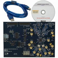
Manufacturer Part Number
AD9958/PCB
Description
BOARD EVALUATION FOR AD9958
Manufacturer
Analog Devices Inc
Datasheet
1.AD9958BCPZ.pdf
(44 pages)
Specifications of AD9958/PCB
Design Resources
Low Jitter Sampling Clock Generator for High Performance ADCs Using AD9958/9858 and AD9515 (CN0109) Phase Coherent FSK Modulator (CN0186)
Lead Free Status / RoHS Status
Contains lead / RoHS non-compliant
Available stocks
Company
Part Number
Manufacturer
Quantity
Price
Company:

Part Number:
AD9958/PCBZ
Manufacturer:
Analog Devices Inc
Quantity:
135


AD9958
Each set of communication cycles does not require an I/O update
to be issued. The I/O update transfers data from the I/O port
buffer to active registers. The I/O update can be sent for each
communication cycle or can be sent when all serial operations
are complete. However, data is not active until an I/O update is
sent, with the exception of the channel enable bits in the channel
select register (CSR). These bits do not require an I/O update to
be enabled.
INSTRUCTION BYTE DESCRIPTION
The instruction byte contains the following information:
MSB
D7
R/W
1
Bit D7 of the instruction byte (R/ W ) determines whether a read
or write data transfer occurs after the instruction byte write. A
logic high indicates a read operation. A logic low indicates a
write operation.
Bit D4 to Bit D0 of the instruction byte determine which register is
accessed during the data transfer portion of the communication
cycle. The internal byte addresses are generated by the AD9958.
SERIAL I/O PORT PIN DESCRIPTION
Serial Data Clock (SCLK)
The serial data clock pin is used to synchronize data to and
from the internal state machines of the AD9958. The maximum
SCLK toggle frequency is 200 MHz.
Chip Select ( CS )
The chip select pin allows more than one AD9958 device to be
on the same set of serial communications lines. The chip select
is an active low enable pin. SDIO_x inputs go to a high imped-
ance state when CS is high. If CS is driven high during any
communication cycle, that cycle is suspended until CS is
reactivated low. The CS pin can be tied low in systems that
maintain control of SCLK.
Serial Data I/O (SDIO_x)
Of the four SDIO pins, only the SDIO_0 pin is a dedicated SDIO
pin. SDIO_1, SDIO_2, and SDIO_3 can also be used to ramp
up/ramp down the output amplitude. Bits[2:1] in the channel
select register (CSR, Register 0x00) control the configuration
of these pins. See the Serial I/O Modes of Operation for more
information.
SERIAL I/O PORT FUNCTION DESCRIPTION
Serial Data Out (SDO)
The SDO function is available in single-bit (3-wire) mode only.
In SDO mode, data is read from the SDIO_2 pin for protocols
that use separate lines for transmitting and receiving data (see
Table 26 for pin configuration options). Bits[2:1] in the channel
select register (CSR, Register 0x00) control the configuration of
x = don’t care bit.
D6
x
1
D5
x
1
D4
A4
D3
A3
D2
A2
D1
A1
D0
LSB
A0
Rev. A | Page 32 of 44
this pin. The SDO function is not available in 2-bit or 4-bit serial
I/O modes.
SYNC_I/O
The SYNC_I/O function is available in 1-bit and 2-bit modes.
SDIO_3 serves as the SYNC_I/O pin when this function is
active. Bits CSR[2:1] control the configuration of this pin.
Otherwise, the SYNC_I/O function is used to synchronize the
I/O port state machines without affecting the addressable register
contents. An active high input on the SYNC_I/O (SDIO_3) pin
causes the current communication cycle to abort. After SDIO_3
returns low (Logic 0), another communication cycle can begin,
starting with the instruction byte write. The SYNC_I/O function is
not available in 4-bit serial I/O mode.
MSB/LSB TRANSFER DESCRIPTION
The AD9958 serial port can support both most significant bit
(MSB) first or least significant bit (LSB) first data formats. This
functionality is controlled by CSR[0]. MSB first is the default
mode. When CSR[0] is set high, the AD9958 serial port is in
LSB first format. The instruction byte must be written in the
format indicated by CSR[0], that is, if the AD9958 is in LSB first
mode, the instruction byte must be written from LSB to MSB. If
the AD9958 is in MSB first mode (default), the instruction byte
must be written from MSB to LSB.
Example Operation
To write Function Register 1 (FR1, Register 0x01) in MSB first
format, apply an instruction byte of 00000001 starting with the
MSB (in the following example instruction byte, the MSB is
D7). From this instruction, the internal controller recognizes a
write transfer of three bytes starting with the MSB, FR1[23].
Bytes are written on each consecutive rising SCLK edge until
Bit 0 is transferred. When the last data bit is written, the I/O
communication cycle is complete and the next byte is considered
an instruction byte.
Example Instruction Byte
MSB
D7
0
1
To write Function Register 1 (FR1) in LSB first format, apply an
instruction byte of 00000001, starting with the LSB bit (in the
preceding example instruction byte, the LSB is D0). From this
instruction, the internal controller recognizes a write transfer of
three bytes, starting with the LSB, FR1[0]. Bytes are written on
each consecutive rising SCLK edge until Bit 23 is transferred.
When the last data bit is written, the I/O communication cycle is
complete and the next byte is considered an instruction byte.
Note that the bit values are for example purposes only.
D6
0
D5
0
D4
0
1
D3
0
D2
0
D1
0
LSB
D0
1
Related parts for AD9958/PCB
Image
Part Number
Description
Manufacturer
Datasheet
Request
R

Part Number:
Description:
BOARD EVALUATION FOR AD9958
Manufacturer:
Analog Devices Inc
Datasheet:


Part Number:
Description:
±1.7g Dual-Axis IMEMS Accelerometer Evaluation Board
Manufacturer:
Analog Devices Inc
Datasheet:

Part Number:
Description:
Inertial Sensor Evaluation System
Manufacturer:
Analog Devices Inc
Datasheet:
Part Number:
Description:
Manufacturer:
Analog Devices Inc
Datasheet:
Part Number:
Description:
Manufacturer:
Analog Devices Inc
Datasheet:
Part Number:
Description:
Manufacturer:
Analog Devices Inc
Datasheet:
Part Number:
Description:
Manufacturer:
Analog Devices Inc
Datasheet:
Part Number:
Description:
Manufacturer:
Analog Devices Inc
Datasheet:
Part Number:
Description:
Manufacturer:
Analog Devices Inc
Datasheet:
Part Number:
Description:
Manufacturer:
Analog Devices Inc
Datasheet:
Part Number:
Description:
Manufacturer:
Analog Devices Inc
Datasheet:
Part Number:
Description:
Manufacturer:
Analog Devices Inc
Datasheet: