ADNK-5033-TN24 Avago Technologies US Inc., ADNK-5033-TN24 Datasheet
ADNK-5033-TN24
Specifications of ADNK-5033-TN24


Related parts for ADNK-5033-TN24


ADNK-5033-TN24 Summary of contents
Page 1
ADNS-5030 Low Power Optical Mouse Sensor Data Sheet Description The Avago Technologies ADNS-5030 is a low power, small form factor optical mouse sensor. It has a new low-power architecture and automatic power management modes, making it ideal for battery, power-sensitive ...
Page 2
Pinout of ADNS-5030 Optical Mouse Sensor Pin Name Description 1 MISO Serial Data Output (Master In/Slave Out) 2 XY_LED LED Control 3 NRESET Reset Pin (active low input) 4 NCS Chip Select (active low input) 5 SCLK Serial Clock Input ...
Page 3
Overview of Optical Mouse Sensor Assembly Avago Technologies provides an IGES file drawing de- scribing the base plate molding features for lens and PCB alignment. The ADNS-5030 sensor is designed for mounting on a through-hole PCB, looking down. There is ...
Page 4
TOP PCB to SURFACE (0.293) (0.417) 2.40 BOTTOM of LENS FLANGE to SURFACE (0.094) DIMENSIONS IN mm (INCHES) Figure 4. 2D Assembly drawing of ADNS-5030 (top and side view). 4 TOP VIEW CROSS SECTION SIDE VIEW SENSOR LENS ...
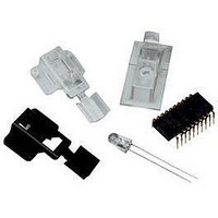
Page 5
ADNS-5200 (LED CLIP) SENSOR CUSTOMER SUPPLIED BASE PLATE WITH RECOMMENDED ALIGNMENT FEATURES PER IGES DRAWING Figure 5. Exploded view drawing. PCB Assembly Considerations 1. Insert the sensor and all other electrical components into PCB. 2. Insert the LED into the ...
Page 6
Design Considerations for Improved ESD Performance For improved electrostatic discharge performance, typical creepage and clearance distance are shown in the table below. Assumption: base plate construction as per the Avago Technologies supplied IGES file and ADNS- 5100/5100-001 lens. Typical Distance ...
Page 7
7 ...
Page 8
Regulatory Requirements x Passes FCC B and worldwide analogous emission limits when assembled into a mouse with shielded cable and following Avago Technologies recommendations. x Passes IEC-1000-4-3 radiated susceptibility level when assembled into a mouse with shielded cable and following ...
Page 9
SENSOR OBJECT SURFACE 2. (0.094) Figure 9. Distance from lens reference plane to tracking surface (Z). AC Electrical Specifications Electrical Characteristics over recommended operating conditions. Typical values at 25 °C, V Parameter Symbol Reset Pulse Width t RESET ...
Page 10
DC Electrical Specifications Electrical Characteristics over recommended operating conditions. Typical values at 25°C, V Parameter Symbol Minimum DC Supply Current I DD_AVG_HIGH in Various Mode I DD_AVG_LOW I DD_REST1 I DD_REST2 I DD_REST3 Power Down Input Low Voltage V IL ...
Page 11
Power Management Modes The ADNS-5030 has three power-saving modes. Each mode has a different motion detection period, affecting response time to mouse motion (Response Time). The sensor automatically changes to the appropriate mode, depending on the time since the last ...
Page 12
SCLK MOSI t hold, MOSI t setup, MOSI MOSI Setup and Hold Time Read Operation A read operation, defined as data going from the ADNS- 5030 to the micro-controller, is always initiated by the micro-controller and consists of two bytes. ...
Page 13
Required Timing between Read and Write Commands There are minimum timing requirements between read and write commands on the serial port. SCLK ADDRESS DATA WRITE OPERATION Timing between Two Write Commands If the rising edge of the SCLK for the ...
Page 14
Motion Burst Timing SCLK MOTION_BURST REGISTER ADDRESS READ FIRST BYTE FIRST READ OPERATION Burst Mode Operation Burst mode is a special serial port operation mode that may be used to reduce the serial transaction time for a motion read. The ...
Page 15
Registers The ADNS-5030 registers are accessible via the serial port. The registers are used to read motion data and status as well as to set the device configuration. Address Register 0x00 Product_ID 0x01 Revision_ID 0x02 Motion 0x03 Delta_X 0x04 Delta_Y ...
Page 16
Product_ID Address: 0x00 Access: Read Reset Value: 0x11 Bit 7 Field PID 7 Data Type: 8-Bit unsigned integer USAGE: This register contains a unique identification assigned to the ADNS-5030. The value in this register does not change; it can be ...
Page 17
Delta X Address: 0x03 Access: Read Reset Value: 0x00 Bit 7 Field X 7 Data Type: Eight bit 2’s complement number USAGE: X movement is counts since last report. Absolute value is determined by resolution. Reading clears the register. MOTION ...
Page 18
Squal Address: 0x05 Access: Read Reset Value: 0x00 Bit 7 Field SQ 7 Data Type: Upper 8 bits of a 9-bit unsigned integer USAGE: SQUAL (Surface Quality measure of the number of valid features visible by the sensor ...
Page 19
Shutter_Upper Address: 0x06 Access: Read Reset Value: 0x00 Bit 7 Field S 15 Shutter_Lower Address: 0x07 Access: Read Reset Value: 0x00 Bit 7 Field S 7 Data Type: Sixteen bit unsigned integer USAGE: Units are clock cycles. Read Shutter_Upper first, ...
Page 20
Maximum_Pixel Address: 0x08 Access: Read Reset Value: 0x00 Bit 7 Field MP 0 Data Type: Eight-bit number USAGE: Maximum Pixel value in current frame. Minimum value = 0, maximum value = 127. The maximum pixel value can vary with every ...
Page 21
Pixel_Grab Address: 0x0b Access: Read/Write Reset Value: 0x00 Bit 7 Field Valid Data Type: Eight-bit word USAGE: The pixel grabber captures 1 pixel per frame. If there is a valid pixel in the grabber when this register is read, the ...
Page 22
Reserved Address: 0x0c Mouse_control Address: 0x0d Access: Read/Write Reset Value: 0x00 Bit 7 Field Reserved Reserved Reserved Reserved Data Type: Eight bit number USAGE: Mouse sensor resolution and power down settings can be accessed edited by this ...
Page 23
Sensor_Current_Setting Address: 0x40 Access: Write Reset Value: N/A Bit 7 Field Reserved Reserved Reserved Reserved Data Type: 8-bit number USAGE: This register is used to set the internal LED driver’s drive strength. Field Name LDC Reserved Reserved Address: 0x41-0x44 Rest_mode_configuration ...
Page 24
Reserved Address: 0x46-0x62 Motion_Burst Address: 0x63 Access: Read Reset Value: 0x00 Bit 7 Field MB 7 Data Type: Various USAGE: Read from this register to activate burst mode. The sensor will return the data in the Delta_X, Delta_Y, Squal, Shutter_Upper, ...