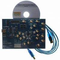
AD9549/PCBZ Analog Devices Inc, AD9549/PCBZ Datasheet - Page 18
AD9549/PCBZ
Manufacturer Part Number
AD9549/PCBZ
Description
BOARD EVALUATION FOR AD9549
Manufacturer
Analog Devices Inc
Datasheet
1.AD9549ABCPZ.pdf
(76 pages)
Specifications of AD9549/PCBZ
Main Purpose
Timing, Clock Generator
Embedded
No
Utilized Ic / Part
AD9549
Primary Attributes
2 Inputs, 2 Outputs, VCO
Secondary Attributes
CMOS, HSTL Output Logic, Graphical User Interface
Lead Free Status / RoHS Status
Lead free / RoHS Compliant


AD9549
The PFD outputs a time series of digital words that are routed
to the digital loop filter. The digital filter implementation offers
many advantages: The filter response is determined by numeric
coefficients rather than by discrete component values; there is
no aging of components and, therefore, no drift of component
value over time; there is no thermal noise in the loop filter; and
there is no control node leakage current (which causes reference
feedthrough in a traditional analog PLL).
The output of the loop filter is a time series of digital words.
These words are applied to the frequency tuning input of a DDS
to steer the DCO frequency. The DDS provides an analog output
signal via an integrated DAC, effectively mimicking the operation
of an analog voltage-controlled oscillator (VCO).
The DPLLC can be programmed to operate in conjunction with
an internal frequency estimator to help decrease the time required
to achieve lock. When the frequency estimator is employed,
frequency acquisition is accomplished in the following two-
step process:
1.
2.
As mentioned in Step 1, the DPLLC includes a feedback divider
that allows the DCO to operate at an integer multiple (S) of f
This establishes a nominal DCO frequency (f
INPUT
Feedforward Divider (Divide-by-R)
The feedforward divider is an integer divider that allows
frequency prescaling of the REF source input signal while
maintaining the desired low jitter performance of the AD9549.
The feedforward divider is a programmable modulus divider with
very low jitter injection. The divider is capable of handling input
frequencies as high as 750 MHz. The divider depth is 16 bits,
REF
÷R
An estimate is made of the frequency of f
lock control loop is essentially inoperative during the
frequency estimation process. When a frequency estimate
is made, it is delivered to the DDS so that its output frequency
is approximately equal to f
of the feedback divider).
The phase lock control loop becomes active and acts as
a servo to acquire and hold phase lock with the reference
signal.
CLK
f
DDS
CONVERTER)
DETECTOR
=
(TIME-TO-
DIGITAL
PHASE
÷PFD
DIV
R
S
Figure 23. Digital PLL Block Diagram
f
÷S
R
DELIVERED AT
THE CLK RATE
SAMPLES
α β
FILTER
LOOP
PFD
FDBK_IN
PINS
÷P
ץ
multiplied by S (the modulus
CCI
DELIVERED AT
SYSCLK RATE
SAMPLES
RECONSTRUCTION
EXTERNAL DAC
DDS
FILTER
PFD
), given by
. The phase
DDS
SYSCLK
DAC_OUT
PINS
Rev. D | Page 18 of 76
PFD
.
cascaded with an additional divide-by-2. Therefore, the divider
is capable of integer division from 1 to 65,535 (index of 1) or from
2 to 131,070 (index of 2). The divider is programmed via the I/O
register map to trigger on either the rising (default) or falling edge
of the REF source input signal. Note that the value stored in the
R-divider register is one less than the actual R-divider, so setting the
R-divider register to 0 results in an R-divider that is equal to 1.
There is a lower bound on the value of R that is imposed by the
phase frequency detector within the DPLLC, which has a maxi-
mum operating frequency of f
Phase Detector section. The R-divider/2 bit must be set when
REFA or REFB is greater than 400 MHz. The user must also
ensure that R is chosen so that it satisfies the inequality.
The upper bound is
where the ceil(x) function yields the nearest integer ≥ x.
For example, if f
ceil (155/24.5) = 7, so R must be ≥7.
Feedback Divider (Divide-by-S)
The feedback divider is an integer divider allowing frequency
multiplication of the REF signal that appears at the input of the
phase detector. It is capable of handling frequencies well above
the Nyquist limit of the DDS. The divider depth is 16 bits, cas-
caded with an additional divide-by-2. Therefore, the divider is
capable of integer division from 1 to 65,535 (index of 1) or from
2 to 131,070 (index of 2). The divider is programmed via the I/O
register map to trigger on either the rising (default) or falling
edge of the feedback signal. Note that the value stored in the
S-divider register is one less than the actual R-divider, so setting
the S-divider register to 0 results in an S-divider equal to 1.
The feedback divider must be programmed within certain
boundaries. The S-divider/2 bit must be set when FDBK_IN is
greater than 400 MHz. The upper boundary on the feedback
divider is the lesser of the maximum programmable value of
S and the maximum practical output frequency of the DDS
(~40% f
index of 1 and S
or
where R is the modulus of the feedforward divider, f
sample rate, and f
S
S
R
R
MAX1
MAX
≥
≤
S
). Two equations are given: S
ceil
floor
2
=
=
min
min
f
MAX2
R
PFD
8
R
= 155 MHz and f
kHz
f
f
is the input reference frequency.
[
R
R
40
MAX
40
for an index of 2.
%
%
f
]
f
R
f
R
f
S
S
R
R
,
,
65
PFD[MAX]
131
,
535
,
070
PFD[MAX]
, as explained in the Fine
MAX1
for a feedback divider
= 24.5 MHz, then
S
is the DAC
Related parts for AD9549/PCBZ
Image
Part Number
Description
Manufacturer
Datasheet
Request
R


Part Number:
Description:
±1.7g Dual-Axis IMEMS Accelerometer Evaluation Board
Manufacturer:
Analog Devices Inc
Datasheet:

Part Number:
Description:
Inertial Sensor Evaluation System
Manufacturer:
Analog Devices Inc
Datasheet:
Part Number:
Description:
Manufacturer:
Analog Devices Inc
Datasheet:
Part Number:
Description:
Manufacturer:
Analog Devices Inc
Datasheet:
Part Number:
Description:
Manufacturer:
Analog Devices Inc
Datasheet:
Part Number:
Description:
Manufacturer:
Analog Devices Inc
Datasheet:
Part Number:
Description:
Manufacturer:
Analog Devices Inc
Datasheet:
Part Number:
Description:
Manufacturer:
Analog Devices Inc
Datasheet:
Part Number:
Description:
Manufacturer:
Analog Devices Inc
Datasheet:
Part Number:
Description:
Manufacturer:
Analog Devices Inc
Datasheet:
Part Number:
Description:
Manufacturer:
Analog Devices Inc
Datasheet:
Part Number:
Description:
Manufacturer:
Analog Devices Inc
Datasheet: