AD9549/PCBZ Analog Devices Inc, AD9549/PCBZ Datasheet - Page 3
AD9549/PCBZ
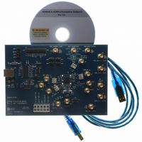
Manufacturer Part Number
AD9549/PCBZ
Description
BOARD EVALUATION FOR AD9549
Manufacturer
Analog Devices Inc
Datasheet
1.AD9549ABCPZ.pdf
(76 pages)
Specifications of AD9549/PCBZ
Main Purpose
Timing, Clock Generator
Embedded
No
Utilized Ic / Part
AD9549
Primary Attributes
2 Inputs, 2 Outputs, VCO
Secondary Attributes
CMOS, HSTL Output Logic, Graphical User Interface
Lead Free Status / RoHS Status
Lead free / RoHS Compliant


REVISION HISTORY
12/10—Rev. C to Rev. D
Changes to I
Pin44, Pin 45) Parameter ................................................................. 4
Changes to Total Power Dissipation Parameter and Added
Endnote 4 ........................................................................................... 5
Changes to Pin 59 Description ...................................................... 11
Changes to Direct Digital Synthesizer (DDS) Section ............... 20
Changes to Power-Up Section ....................................................... 42
Changes to Address 0x0002 Default Value (in Table 13) ........... 48
Changes to Address 0x0400 and Address 0x40E Default Values
(in Table 13) ..................................................................................... 52
5/10—Rev. B to Rev. C
Deleted 64-Lead LFCSP (CP-64-1) .................................. Universal
Changes to SYSCLK PLL Enabled/Minimum Differential Input
Level Parameter, Table 2 ................................................................... 6
Updated Outline Dimensions ........................................................ 74
Changes to Ordering Guide ........................................................... 74
1/10—Rev. A to Rev. B
Changes to I/O Register Map Section, Introduction and
Table 13 ............................................................................................. 48
Changes to Register 0x0405 to Register 0x0408—Reserved
Section .............................................................................................. 70
Added Register 0x0406—Part Version Section ........................... 71
AVDD
(Pin 19, Pin 23 to Pin 26, Pin 29, Pin 30,
Rev. D | Page 3 of 76
12/09—Rev. 0 to Rev. A
Added 64-Lead LFCSP (CP-64-7) ................................... Universal
Changes to Total Power Dissipation Parameter ............................ 5
Changes to Serial Port Timing Specifications and
Propagation Delay Parameters ........................................................ 8
Added Exposed Paddle Notation to Figure 2; Changes to
Table 4 ............................................................................................... 10
Corrected DDS Phase Offset Resolution from 16 Bits to
14 Bits Throughout; Change to Figure 25 .................................... 20
Changes to Phase Lock Detection Section .................................. 24
Change to Figure 30 ........................................................................ 25
Changes to Loss of Reference and Reference Frequency
Monitor Sections ............................................................................. 26
Change to Output Frequency Range Control Section ............... 32
Change to Figure 46 ........................................................................ 36
Changes to Frequency Estimator Section .................................... 37
Changes to Programming Sequence Section .............................. 42
Changes to Power Supply Partitioning Section ........................... 43
Change to Serial Control Port Section ......................................... 44
Changes to Figure 54 ...................................................................... 46
Added Exposed Paddle Notation to Outline Dimensions and
Changes to Ordering Guide ........................................................... 74
8/07—Revision 0: Initial Version
AD9549
Related parts for AD9549/PCBZ
Image
Part Number
Description
Manufacturer
Datasheet
Request
R


Part Number:
Description:
±1.7g Dual-Axis IMEMS Accelerometer Evaluation Board
Manufacturer:
Analog Devices Inc
Datasheet:

Part Number:
Description:
Inertial Sensor Evaluation System
Manufacturer:
Analog Devices Inc
Datasheet:
Part Number:
Description:
Manufacturer:
Analog Devices Inc
Datasheet:
Part Number:
Description:
Manufacturer:
Analog Devices Inc
Datasheet:
Part Number:
Description:
Manufacturer:
Analog Devices Inc
Datasheet:
Part Number:
Description:
Manufacturer:
Analog Devices Inc
Datasheet:
Part Number:
Description:
Manufacturer:
Analog Devices Inc
Datasheet:
Part Number:
Description:
Manufacturer:
Analog Devices Inc
Datasheet:
Part Number:
Description:
Manufacturer:
Analog Devices Inc
Datasheet:
Part Number:
Description:
Manufacturer:
Analog Devices Inc
Datasheet:
Part Number:
Description:
Manufacturer:
Analog Devices Inc
Datasheet:
Part Number:
Description:
Manufacturer:
Analog Devices Inc
Datasheet: