27100 Parallax Inc, 27100 Datasheet - Page 10
27100
Manufacturer Part Number
27100
Description
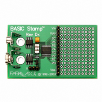
BASIC STAMP REV DX MODULE
Manufacturer
Parallax Inc
Type
Microcontrollerr
Datasheet
1.27100.pdf
(23 pages)
Specifications of 27100
Contents
Board
Product
Microcontroller Basic Stamps
Operating Supply Voltage
5 to 15 V
Board Size
63.5 mm x 38.1 mm x 12.7 mm
For Use With/related Products
BASIC Stamp®
Lead Free Status / RoHS Status
Lead free / RoHS Compliant
Available stocks
Company
Part Number
Manufacturer
Quantity
Price

Part Number:
271000-51300730
Manufacturer:
DENSO
Quantity:
20 000


STAMP FAQS
What is the VIN pin used for?
How does the VDD pin work?
How does the reset pin (RES) work?
How does the ATN (Attention) pin work (BASIC Stamp II, BASIC STAMP IIe and BASIC
Stamp IIsx)?
Last Revised On: 7/21/00
The VIN (Voltage Input) pin is used to power the BASIC Stamp from a 6 to 15 volt source. The VIN pin is the
positive connection while the VSS pin is the negative, or ground, connection. When powered from the VIN pin the
BASIC Stamp regulates the voltage down and outputs +5 volts on the VDD pin. For optimal operation, it is
recommended to keep the voltage below 12 volts for the BASIC Stamp I and II, IIe, and around 7.5 volts for the
BASIC Stamp IIsx.
The VDD pin (+5V) outputs 5 volts when the BASIC Stamp is powered by a 6 to 15 volt source using the VIN
and VSS (ground) pins. The VDD pin can be used to power other circuitry if the overall current consumption is
within the capabilities of the BASIC Stamp’s regulator. The VDD pin can also be used to power the BASIC
Stamp from an external 5-volt regulator. In this case, the VDD pin is the +5 volt connection and the VSS (ground)
pin is the negative connection of the regulator.
The reset pin is internally controlled by the BASIC Stamp’s brownout detector. It is normally high (+5V), which
allows the BASIC Stamp to run its program normally, and is pulled low when the power supply voltage drops
below 4 volts (safely putting the BASIC Stamp to sleep). This pin can be monitored to detect when a reset
condition occurs, or, you can pull the line to ground to force a reset. After the reset pin is allowed to rise to +5
volts, the BASIC Stamp wakes up and starts executing its program from the first line of code. Do not drive this pin
high, it should be left electrically disconnected (floating) when you want the BASIC Stamp to run normally. This pin
has an inverse relationship to the ATN (Attention) pin on the BASIC Stamp II, BASIC STAMP IIe and BASIC
Stamp IIsx.
The ATN pin is used strictly for programming the BASIC Stamp II, BASIC STAMP IIe, or BASIC Stamp IIsx,
and should not be connected to anything other than the DTR pin of the programming connector and/or filtering
capacitors. The ATN pin is an input and has an inverse relationship with the reset (RES) pin. When the ATN pin is
left unconnected, or is driven low, it causes the RES pin to go high (allowing the BASIC Stamp II, IIe or IIsx to
function properly). When the ATN pin is driven high it causes the RES pin to go low (performing a hardware reset
on the BASIC Stamp II, IIe or IIsx). The BASIC Stamp editor software toggles this pin from low to high and then
low again at the start of the programming process to perform a hardware reset on the module and begin the bi-
directional programming communication. It is important to be aware of a particular artifact of the DTR pin on a
standard serial port: upon port selection by standard software (terminal packages, development tools, etc.), the
DTR pin is driven high by default. If the same connections for programming the BASIC Stamp II, IIe or IIsx are
used to communicate with it via a serial port, the default state of the DTR pin will cause the BASIC Stamp to be
held in permanent reset and its PBASIC program will not execute. (This is the case on the Stamp II Carrier
Board). This problem can be fixed in a number of ways: 1) disconnect the DTR to ATN pin connection when trying
to communicate serially to the BASIC Stamp, or 2) explicitly set the DTR pin to low after selecting the port if the
terminal package or development tool allows this, or 3) modify the programming connection to include a 0.1 Fu
capacitor in series with the DTR to ATN pin connection and a 0.1 Fu capacitor from ATN to ground (VSS). The
last two options will allow you to use the same connection for both programming and serial communications. (The
Super Carrier Board, BASIC Stamp Activity Board and Board of Education use the last method).
PROGRAMMING INFORMATION
Page: 10
Related parts for 27100
Image
Part Number
Description
Manufacturer
Datasheet
Request
R


Part Number:
Description:
Microcontroller Modules & Accessories DISCONTINUED BY PARALLAX
Manufacturer:
Parallax Inc

Part Number:
Description:
BOOK UNDERSTANDING SIGNALS
Manufacturer:
Parallax Inc
Datasheet:


Part Number:
Description:
COMPETITION RING FOR SUMOBOT
Manufacturer:
Parallax Inc
Datasheet:


Part Number:
Description:
TEXT INFRARED REMOTE FOR BOE-BOT
Manufacturer:
Parallax Inc
Datasheet:
Part Number:
Description:
BOARD EXPERIMENT+LCD NX-1000
Manufacturer:
Parallax Inc
Datasheet:

Part Number:
Description:
CONTROLLER 16SERVO MOTOR CONTROL
Manufacturer:
Parallax Inc
Datasheet:

Part Number:
Description:
BASIC STAMP LOGIC ANALYZER
Manufacturer:
Parallax Inc
Datasheet:

Part Number:
Description:
IC MCU 2K FLASH 50MHZ SO-18
Manufacturer:
Parallax Inc
Datasheet: