27100 Parallax Inc, 27100 Datasheet - Page 18
27100
Manufacturer Part Number
27100
Description
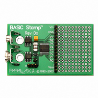
BASIC STAMP REV DX MODULE
Manufacturer
Parallax Inc
Type
Microcontrollerr
Datasheet
1.27100.pdf
(23 pages)
Specifications of 27100
Contents
Board
Product
Microcontroller Basic Stamps
Operating Supply Voltage
5 to 15 V
Board Size
63.5 mm x 38.1 mm x 12.7 mm
For Use With/related Products
BASIC Stamp®
Lead Free Status / RoHS Status
Lead free / RoHS Compliant
Available stocks
Company
Part Number
Manufacturer
Quantity
Price

Part Number:
271000-51300730
Manufacturer:
DENSO
Quantity:
20 000


STAMP FAQS
How do I input or output data in parallel on the I/O pins?
Why do the BASIC Stamp’s output pins toggle briefly when I use the SLEEP, NAP or END
commands or allow my program to end naturally?
Last Revised On: 7/21/00
All BASIC Stamps have predefined variables that refer to the I/O pins. On the BASIC Stamp I, the PINS variable
refers to all eight I/O pins. Thus code such as:
would copy the current state of all I/O pins (an 8-bit byte) into the variable Snapshot. Similarly:
would set the eight output pins to the binary form of 150, or %10010110.
On the BASIC Stamp II, IIe and IIsx, the PINS variable was replaced with the INS and OUTS variables. Both
INS and OUTS refer to all sixteen pins, while their derivatives, INL, INH, OUTL and OUTH refer to the low and
high bytes (groups of 8 pins). For example, the following code will input 8-bits in parallel from the lower 8 pins:
The following code will output 8-bits in parallel from the upper 8 pins:
Inside the BASIC Stamp’s interpreter chip is a watchdog timer whose main purpose is to reset the interpreter chip
if, for some reason, it should stop functioning properly. The SLEEP and NAP commands also utilize the watchdog
timer to periodically (every 2.3 seconds to be exact) “wake-up” the BASIC Stamp from its low-power mode.
Upon reset, the I/O pins are set to inputs for approximately 18 mS before returning to their previous directions and
states. If you have an output pin set to a logical 1 state (+5V) and you use the SLEEP command, every 2.3
seconds during sleep mode that I/O pin will switch to an input for 18 mS causing a momentary signal loss. This
“power glitch” is easily viewable with an LED and a 470 ohm resister tied to an I/O pin and switched on just before
entering sleep mode. In many cases this problem can be remedied by tying a pull-up or pull-down resistor to the
I/O pin in question to provide a constant source of power should the I/O pin change directions. Allowing a
PBASIC program to end naturally, or using the END command, will exhibit the same “power glitch” behavior
because the interpreter chip enters a low-power state. The BASIC Stamp II, IIe and IIsx includes the STOP
command which acts just like END, except the output pins remain driven.
SYMBOL Snapshot = B0
Snapshot = PINS
DIRS = %11111111 ‘Set all eight pins as outputs
PINS = 150
Snapshot
Snapshot = INL
DIRS = %1111111100000000 ‘Set upper 8 pins to outputs
OUTH = 255
VAR
BYTE
PROGRAMMING INFORMATION
Page: 18
Related parts for 27100
Image
Part Number
Description
Manufacturer
Datasheet
Request
R


Part Number:
Description:
Microcontroller Modules & Accessories DISCONTINUED BY PARALLAX
Manufacturer:
Parallax Inc

Part Number:
Description:
BOOK UNDERSTANDING SIGNALS
Manufacturer:
Parallax Inc
Datasheet:


Part Number:
Description:
COMPETITION RING FOR SUMOBOT
Manufacturer:
Parallax Inc
Datasheet:


Part Number:
Description:
TEXT INFRARED REMOTE FOR BOE-BOT
Manufacturer:
Parallax Inc
Datasheet:
Part Number:
Description:
BOARD EXPERIMENT+LCD NX-1000
Manufacturer:
Parallax Inc
Datasheet:

Part Number:
Description:
CONTROLLER 16SERVO MOTOR CONTROL
Manufacturer:
Parallax Inc
Datasheet:

Part Number:
Description:
BASIC STAMP LOGIC ANALYZER
Manufacturer:
Parallax Inc
Datasheet:

Part Number:
Description:
IC MCU 2K FLASH 50MHZ SO-18
Manufacturer:
Parallax Inc
Datasheet: