DK-NIOS-2C35N Altera, DK-NIOS-2C35N Datasheet
DK-NIOS-2C35N
Specifications of DK-NIOS-2C35N
DK-NIOS-2C35N
Available stocks


Related parts for DK-NIOS-2C35N


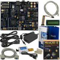
DK-NIOS-2C35N Summary of contents
Page 1
... Cyclone II Edition Reference Manual 101 Innovation Drive San Jose, CA 95134 www.altera.com Nios Development Board Development Board Version Document Version Document Date 6XX-40020R 1.3 May 2007 ...
Page 2
... Altera Corporation in the U.S. and other countries. All other product or service names are the property of their respective holders. Al- tera products are protected under numerous U ...
Page 3
... About this Manual................................................................................... v How to Contact Altera .............................................................................................................................. v Typographic Conventions ...................................................................................................................... vi Chapter 1. Overview Features Overview ................................................................................................................................. 1–1 General Description ............................................................................................................................... 1–1 Factory-Programmed Reference Design ............................................................................................ 1–2 Chapter 2. Board Components Component List ...................................................................................................................................... 2–1 Cyclone II EP2C35 Device (U62) ......................................................................................................... 2–3 Push-Button Switches (SW0 - SW3) .................................................................................................... 2–4 Individual LEDs (D0 - D7) .................................................................................................................... 2–5 Seven-Segment LEDs (U8 & U9) ........................................................................................................ 2–5 SSRAM Chip (U74) ................................................................................................................................ 2– ...
Page 4
... Appendix B. Connecting to the Board via Ethernet Introduction ........................................................................................................................................... B–1 Connecting the Ethernet Cable ........................................................................................................... B–1 Connecting the LCD Screen ........................................................................................................... B–2 Obtaining an IP Address ................................................................................................................ B–2 LAN Connection ....................................................................................................................... B–3 DHCP .................................................................................................................................... B–3 Static IP Address .................................................................................................................. B–3 Point–to–Point Connections .................................................................................................... B–4 Browsing to Your Board ...................................................................................................................... B–5 iv Nios Development Board Cyclone II Edition Altera Corporation ...
Page 5
... The table shows this document’s revision history. Date & Revision May 2007, 1.3 October 2006, 1.2 June 2006, 1.1 May 2005, 1.0 How to Contact For the most up-to-date information about Altera products, refer to the following table. Altera Technical support Technical training Altera Corporation May 2007 ...
Page 6
... Nios Development Board Cyclone II Edition Contact Contact (1) Method Website Email Email Email (Software Licensing) You can also contact your local Altera sales office or sales representative. Meaning , \qdesigns directory, d: drive, chiptrip.gdf file. MAX , PIA input. , Active-low signals are denoted by suffix c:\qdesigns\tutorial\chiptrip.gdf SUBDESIGN ), as well as logic function names (e ...
Page 7
... The warning indicates information that should be read prior to starting or w continuing the procedure or processes r The angled arrow indicates you should press the Enter key. f The feet direct you to more information on a particular topic. Altera Corporation May 2007 Meaning Reference Manual Nios Development Board Cyclone II Edition About this Manual vii ...
Page 8
... About this Manual viii Nios Development Board Cyclone II Edition Reference Manual Altera Corporation May 2007 ...
Page 9
... RS-232 DB9 serial port Four push-button switches connected to FPGA user I/O pins Eight LEDs connected to FPGA user I/O pins Dual 7-segment LED display JTAG connectors to Altera devices via Altera download cables 50 MHz oscillator and zero-skew clock distribution circuitry Power-on reset circuitry 1. Overview ® ...
Page 10
... Nios Development Board Cyclone II Edition 1–1shows a block diagram of the Nios development board. 16 Mbyte DDR SDRAM 2 Mbyte SSRAM Vccint 1.2-V EPCS64 Configuration Vccio 3.3-V Configuration 27 Cyclone II EP2C35 FPGA 41 PMC Connector Reference Manual Device Controller 16 Mbyte Flash Memory Ethernet RJ45 MAC/PHY Connector RS-232 Altera Corporation May 2007 ...
Page 11
... In the course of development, you might overwrite or erase the flash memory space containing the default reference design. Altera provides the flash image for the default reference design so you can return the board to its default state. Refer to Appendix A: Restoring the Factory Configuration for more information. ...
Page 12
... Overview 1–4 Nios Development Board Cyclone II Edition Reference Manual Altera Corporation May 2007 ...
Page 13
... Table 2–1. Nios Development Board, Cyclone II Edition Components & Interfaces Board Designation U62 Cyclone II FPGA User Interface SW0 – SW3 Push-button switches D0 – D7 Individual LEDs U8, U9 Seven-segment LEDs Altera Corporation May 2007 2. Board Components Figure 2–1 J26 J19 Optional Power Optional Power Optional Power Supply Supply ...
Page 14
... Test Points J24 JTAG connector J5 JTAG connector J27 EPCS configuration header Configuration & Reset U3 MAX Configuration controller Altera MAX EPM7256AE device used to configure U69 Serial configuration device SW8 CPU Reset button 2–2 Nios Development Board Cyclone II Edition Name 2 Mbytes of synchronous SRAM. ...
Page 15
... M4K Memory Blocks Total RAM Bits Embedded 18x18 Multiplier Blocks PLLs User I/O Pins 1 Altera Corporation May 2007 Name Push-button switch to reconfigure the FPGA with the factory-programmed reference design. Push-button switch to reset the board. LEDs that display the current configuration status of the FPGA ...
Page 16
... The development board provides two separate methods for configuring the FPGA For Cyclone II-related documentation including pin out data for the EP2C35 device, see the Altera Cyclone II literature page at www.altera.com/literature/lit-cyc2.jsp. Push-Button SW0 – SW3 are momentary-contact push-button switches to provide stimulus to designs in the FPGA. Refer to Switches (SW0 - ...
Page 17
... I/O pin. Refer to LEDs (U8 & U9) drives logic 0, the corresponding U8 and U9 LED turns on. See for pin-out details. Figure 2–3. Dual Seven-Segment Display Altera Corporation May 2007 “Push-Button Switches (SW0 - SW3)” on page Table 2–4. When a pin drives logic 0, the corresponding LED ...
Page 18
... Mbyte, 32-bit-wide, zero-wait-state main memory. 2–6 Nios Development Board Cyclone II Edition FPGA Pin U8 & U9 Pin Reference Manual Pin Function Board Net Name a hex_0A b hex_0B c hex_0C d hex_0D e hex_0E f hex_0F g hex_0G dp hex_0DP a hex_1A b hex_1B c hex_1C d hex_1D e hex_1E f hex_1F g hex_1G dp hex_1DP Altera Corporation May 2007 ...
Page 19
... Table 2–6 Table 2–6. SSRAM Pin Table AB3 AB4 L10 Altera Corporation May 2007 shows all connections between the FPGA and the SSRAM chip. FPGA Pin U74 Pin 100 Reference Manual Nios Development Board Cyclone II Edition Board Components Pin Function Board Net Name ...
Page 20
... D28 ssram_d20 D29 ssram_d21 D30 ssram_d22 D31 ssram_d23 D16 ssram_d24 D17 ssram_d25 D18 ssram_d26 D19 ssram_d27 D20 ssram_d28 D21 ssram_d29 D22 ssram_d30 D23 ssram_d31 OE_n ssram_oe_n WE_n ssram_we_n ADSP_n ssram_adsp_n ADV_n ssram_adv_n CE2 ssram_ce2 CE3_n ssram_ce3_n Altera Corporation May 2007 ...
Page 21
... U63 Pin 2 sdram_dq0 4 sdram_dq1 5 sdram_dq2 7 sdram_dq3 8 sdram_dq4 10 sdram_dq5 11 sdram_dq6 13 sdram_dq7 54 sdram_dq8 56 sdram_dq9 57 sdram_dq10 59 sdram_dq11 60 sdram_dq12 62 sdram_dq13 Reference Manual Nios Development Board Cyclone II Edition Board Components Pin Function Board Net Name GW_n ssram_gw_n CLK sram_clk Table 2–7. Altera Board Net Name 2–9 ...
Page 22
... FPGA Pin U63 Pin 63 sdram_dq14 65 sdram_dq15 16 sdram_dqs0 51 sdram_dqs1 20 sdram_dm0 47 sdram_dm1 29 sdram_a0 30 sdram_a1 31 sdram_a2 32 sdram_a3 35 sdram_a4 36 sdram_a5 37 sdram_a6 38 sdram_a7 39 sdram_a8 40 sdram_a9 28 sdram_a10 41 sdram_a11 42 sdram_a12 26 sdram_ba0 27 sdram_ba1 22 sdram_cas_n 44 sdram_cke 24 sdram_cs_n 23 sdram_ras_n 21 sdram_we_n 46 sdram_clk_n 45 sdram_clk_p Reference Manual Board Net Name Altera Corporation May 2007 ...
Page 23
... G13 C15 B15 B16 C16 D15 Altera Corporation May 2007 A Nios II embedded processor implemented on the FPGA can use the flash memory as general-purpose memory and non-volatile storage. The flash memory can hold FPGA configuration data that is used by the configuration controller to load the FPGA at power-up. Refer to “ ...
Page 24
... Reference Manual Board Net Name fe_a15 fe_a16 fe_a17 fe_a18 fe_a19 fe_a20 fe_a21 fe_a22 fe_a23 fe_d0 fe_d1 fe_d2 fe_d3 fe_d4 fe_d5 fe_d6 fe_d7 flash_cs_n flash_oe_n flash_rw_n flash_wp_n flash_byte_n (1) flash_ry_by_n “SW10 – Reset, Altera Corporation May 2007 ...
Page 25
... G18 D18 E18 A19 B19 D20 D14 Y15 AA15 Altera Corporation May 2007 RJ1 Table 2–9 for connections between the FPGA and the MAC/PHY The Ethernet MAC/PHY device shares both address and data connections with the flash memory. U4 Pin Pin Function ...
Page 26
... Board Net Name (1) enet_be_n0 enet_be_n1 enet_be_n2 enet_be_n3 enet_ior_n enet_iow_n fe_a1 fe_a2 fe_a3 fe_a4 fe_a5 fe_a6 fe_a7 fe_a8 fe_a9 fe_a10 fe_a11 fe_a12 fe_a13 fe_a14 fe_a15 fe_d0 fe_d1 fe_d2 fe_d3 fe_d4 fe_d5 fe_d6 fe_d7 fe_d8 fe_d9 fe_d10 fe_d11 fe_d12 Altera Corporation May 2007 ...
Page 27
... J19’s RXD and TXD pins. LEDs are connected to the RXD and TXD signals and visually indicate when data is being transmitted or received. connections between the serial connectors and the FPGA. Altera Corporation May 2007 U4 Pin Pin Function ...
Page 28
... PROTO2 switches: U27, U28, U29, U30 and U31 ● Reference Manual RXD GND DTR TXD DCD IN IN OUT OUT OUT OUT IN OUT RI CTS RTS DSR Board Net Name serial_rxd serial_txd serial_dtr serial_dcd serial_dsr serial_ri serial_cts serial_rts Altera Corporation May 2007 ...
Page 29
... CompactFlash connector (CON3). Designs can use either the PROTO1 connector or the CompactFlash connector See the Altera web site for a list of available expansion daughter cards that can be used with the Nios development board at www.altera.com/devkits. Table PROTO1 expansion headers to the FPGA. Unless otherwise noted, labels indicate FPGA pin numbers... Table 2– ...
Page 30
... J11 proto1_io25 J11 proto1_io26 J11 proto1_io27 J11 proto1_cardsel_n J11 proto1_io28 J12 proto1_io40 J12 proto1_io29 J12 proto1_io30 J12 proto1_io31 J12 proto1_io32 J12 proto1_io33 J12 proto1_io34 J12 proto1_io35 J12 proto1_io36 J12 proto1_io37 J12 proto1_io38 J12 proto1_io39 J13 proto1_osc Altera Corporation May 2007 ...
Page 31
... Table 2–11. PROTO1 Pin Table (Continued) F21 N26 Figure 2–6. PROTO1 Expansion Prototype Connector - J11, J12 & J13 Altera Corporation May 2007 FPGA Pin PROTO1 Pin 11 13 J11 Pin 1 J12 Pin 1 Reference Manual Nios Development Board Cyclone II Edition Board Components Connector ...
Page 32
... Figure 2–7. PROTO1 Pin Information – J11, J12, & J13 J12 Notes to (1) (2) (3) (4) 2–20 Nios Development Board Cyclone II Edition J11 J13 Figure 2–7: Unregulated voltage from DC power supply. Clk from board oscillator. Clk from FPGA. Clk output from PROTO1 card to FPGA. Reference Manual Altera Corporation May 2007 ...
Page 33
... V22 AF23 AE23 AC22 AB21 AD23 AD22 AC21 AD21 AF22 AE22 V18 W19 U17 U18 AF21 AE21 AB20 AC20 AF20 AE20 AD19 AC19 AA17 AA18 W17 AA20 Altera Corporation May 2007 2–12, Figure 2–8 and Figure 2–9 FPGA Pin PROTO2 Pin ...
Page 34
... Board Net Name J16 proto2_io28 J15 proto2_io40 J15 proto2_io29 J15 proto2_io30 J15 proto2_io31 J15 proto2_io32 J15 proto2_io33 J15 proto2_io34 J15 proto2_io35 J15 proto2_io36 J15 proto2_io37 J15 proto2_io38 J15 proto2_io39 J17 proto2_osc J17 proto2_pllclk J17 proto2_clkout J17 Pin 1 Altera Corporation May 2007 ...
Page 35
... CompactFlash The CompactFlash connector header (CON3) enables hardware designs to access a CompactFlash card. Refer to Connector access modes are supported: (CON3) ■ ■ Altera Corporation May 2007 J16 J15 Figure 2–9: Unregulated voltage from DC power supply. Clk from board oscillator. Clk from FPGA. ...
Page 36
... Do not connect cards to PROTO1 and CON3 at the same time. Damage to one or both cards might result. lists connections between CON3 and the FPGA. CON3 Pin Pin Function Reference Manual “Expansion Prototype for details on PROTO1. Board Net Name (1) proto1_io0 proto1_io1 Altera Corporation May 2007 ...
Page 37
... P18 G23 G24 G25 G26 H23 H24 J23 H25 H26 K18 K24 J25 J26 M21 T23 R17 P17 T18 T17 U26 R19 T19 U20 U21 V26 V25 V24 Altera Corporation May 2007 CON3 Pin Pin Function D10 D11 D12 D13 D14 ...
Page 38
... FPGA must first be configured with a design that includes a PMC interface. Damage to either the FPGA or daughter card can result if the FPGA is not configured correctly. Reference Manual Board Net Name (1) proto1_io39 proto1_io40 cf_cs_n cf_atasel_n cf_power (2) cf_present_n proto1_RESET_n (3) Figure 2–11. The PMC Altera Corporation May 2007 ...
Page 39
... Table 2–15 FPGA. Table 2–15. PMC Connector Pin Table L20 L21 Altera Corporation May 2007 Maximum Power 9.5 Watts 15 Watts 45 Watts 1.2 Watts When connecting an external power supply, the fuse for the corresponding voltage should be removed to prevent the two power supplies from interfering with each other. Refer to “ ...
Page 40
... Board Net Name pmc_ad2 pmc_ad3 pmc_ad4 pmc_ad5 pmc_ad6 pmc_ad7 pmc_ad8 pmc_ad9 pmc_ad10 pmc_ad11 pmc_ad12 pmc_ad13 pmc_ad14 pmc_ad15 pmc_ad16 pmc_ad17 pmc_ad18 pmc_ad19 pmc_ad20 pmc_ad21 pmc_ad22 pmc_ad23 pmc_ad24 pmc_ad25 pmc_ad26 pmc_ad27 pmc_ad28 pmc_ad29 pmc_ad30 pmc_ad31 pmc_be_n0 pmc_be_n1 pmc_be_n2 pmc_be_n3 Altera Corporation May 2007 ...
Page 41
... I/O pins and probed at J25. External scopes and logic analyzers can connect to J25 and analyze a large number of signals simultaneously. f For details on Nios II debugging products that use the Mictor connector, see www.altera.com. Altera Corporation May 2007 FPGA Pin JH1 & JH2 Pin 43 JH1 ...
Page 42
... Figure 2–13. Mictor Connector Signaling Mictor Connector 2–30 Nios Development Board Cyclone II Edition shows an example of an in-target system analyzer ISA- J25 below shows connections from the Mictor connector to the JTAG Connector (J24) (J25) 5 Reference Manual FPGA (U62) 40 Altera Corporation May 2007 ...
Page 43
... TP1 – TP8 are test points connected to I/O pins on the FPGA. FPGA designs can route signals to these I/O pins to be probed. TP1 –TP8 also (TP1 – TP8) connect to the configuration controller (U3). Altera Corporation May 2007 shows the pin out information for J25. Unless otherwise noted, FPGA Pin ...
Page 44
... EPCS device. U69 is blank by default. The Quartus II software can program FPGA configuration data (a .pof file) into U69 through an Altera download cable connected to J27. Alternately, software running on a Nios II processor design can write configuration data to U69. ...
Page 45
... See the Serial Configuration Devices chapter in Altera's Configuration Device Handbook for more information about the EPCS64 device. See the EPCS Device Controller Core with Avalon Interface chapter in the Quartus II Handbook, Volume 5: Altera Embedded Peripherals for information about the EPCS serial flash controller component in SOPC Builder. Configuration The configuration controller (U3 Altera MAX 7000 EPM7256AE device ...
Page 46
... This LED is an indicator of the CONFIG_DONE_signal from the FPGA. This LED illuminates when FPGA configuration completes successfully and CONFIG_DONE goes high. This LED is an indicator of the flash_CE_n line. It illuminates when the flash is being accessed and the CE_n line is being asserted. Figure 2–15. Reference Manual Altera Corporation May 2007 ...
Page 47
... Reset, Config (SW10) is the power-on reset button. Refer to When SW10 is pressed, a logic 0 is driven to the power on reset controller (U18). Refer to Whenever SW10 is pressed, the configuration controller attempts to reconfigure the FPGA. Altera Corporation May 2007 2–16. “Power-Supply Circuitry” on page 2–44 Reference Manual ...
Page 48
... PROTO2) Board power-on Pressing the Reset, Config button (SW10). Asserting (driving 0 volts on) the pld_reconfigreq_n input pin of the EPM7256AE device (U3 pin 94) from the FPGA (U62 pin AA14). Pressing the Factory Config button (SW9). Reference Manual SW10 Reset, Config Altera Corporation May 2007 ...
Page 49
... EPCS64, and configures the FPGA with the factory configuration. SW9 provides an escape from a situation in which a valid-but-nonfunctional design is present in user flash memory or the EPCS64. Altera Corporation May 2007 The EPCS64 serial configuration device The user configuration from flash memory ...
Page 50
... Custom FPGA designs can use the flash memory space in any way necessary. Altera recommends that you do not overwrite the factory- programmed flash memory contents. Without a valid factory configuration, the configuration controller may not be able to successfully configure the FPGA ...
Page 51
... JTAG Connector to FPGA (J24) J24 connects to the JTAG pins (TCK, TDI, TDO, TMS, TRST) of the FPGA (U62) as shown in configure the FPGA with a new hardware image via an Altera download cable as shown in Nios II processor JTAG debug module via a download cable connected to the J24 JTAG connector. ...
Page 52
... The pins of J24 are connected directly to pins on J25, and care must be taken so that signal contention does not occur between the two connectors. 2–40 Nios Development Board Cyclone II Edition To Mictor Connector (J25) JTAG Signals JTAG Connector (J24) J24 Reference Manual FPGA (U62) TDI TMS TCK TDO TRST Pin 1 Altera Corporation May 2007 ...
Page 53
... J5 connects to the JTAG pins (TCK, TDI, TDO, TMS, TRST) of the EPM7256AE device (U3). Altera Quartus II software can perform in- system programming (ISP) to reprogram the EPM7256AE device (U3) with a new hardware image via an Altera download cable as shown in Figure 1 Most users never need to reprogram the configuration controller design in the EMP7256AE device ...
Page 54
... Reference Manual sdram_CLK_p sdram_CLK_n DDR SDRAM (U63) sram_CLK SSRAM (U74 tor_CLK Mi c tor (J25) FPGA (U62) PMC_CLK PLLs PMC (JH1 & JH2) proto1_PLLCLK proto1_CLKOUT PROTO1 proto1_OSCCLK proto2_PLLCLK proto2_CLKOUT PROTO2 proto2_OSCCLK cpl d _CLKOSC MAX (U3) Altera Corporation May 2007 ...
Page 55
... PLLs are only dedicated when using the Enhanced PLL. If you use the Fast PLL, the PLL inputs and outputs are interchangeable. For more information on using PLLs in the Cyclone II refer to the data sheet. The factory-programmed configuration controller and Altera- provided reference designs work only with the 50 MHz clock. Reference Manual ...
Page 56
... DDR SDRAM VDD power supply. FPGA VCCIO for pins that interface to DDR SDRAM. 3.3V power for multiple components on the board. 5.0V power for multiple components on the board. Power for the PMC connectors. Power for the PMC connectors. Reference Manual for more Note Altera Corporation May 2007 ...
Page 57
... Altera Corporation May 2007 Appendix A. Factory Configuration Open a Nios II command shell Windows PC, click Windows Start, point to Programs, Altera, Nios II EDS <installed version>, and then click Nios II Command Shell. From the examples directory, change to the factory_recovery directory for your development kit. cd factory_recovery/niosII_cycloneII_2c35 Run the flash-restoration script: ...
Page 58
... In the Programmer, turn on the Program/Configure checkbox, and click Start to reprogram the EPM7256AE device. Press the Factory Config button to perform a power on reset and reconfigure the FPGA from flash memory. You should see the Factory LED turned on and activity on LEDs D0 through D7. Reference Manual Altera Corporation May 2007 ...
Page 59
... RJ45 crossover adapter. Before you connect these Ethernet Cable components, you must decide how you want to use the network features of your board. Select one of the two following connection methods: 1. Altera Corporation May 2007 Appendix B. the Board via Ethernet B–1. This chapter describes how to connect a host computer to the LAN Connection — ...
Page 60
... RJ1 on the Nios development board as shown in Figure B–2. b. Connect the other end of the RJ45 connector directly to the network (Ethernet) port on your host computer. Reference Manual RJ1 Altera Corporation May 2007 ...
Page 61
... You need to obtain a safe IP address in your LAN's subnet from your system administrator. Once you know a safe IP address, you can assign it to your board using the steps below. These steps send IP configuration data to the board via an Altera JTAG download cable, such as the USB-Blaster cable. 1. ...
Page 62
... Press the SW8 button labeled CPU Reset to reboot the Nios II processor and start the web server using the new IP address. The LCD screen displays the static IP address assigned to the board, along with other status messages. “Browsing to Your Board” on page B–5 Reference Manual to continue. Altera Corporation May 2007 ...
Page 63
... IP address of the board (four numbers separated by decimal-points URL directly into the browser’s Address input field. You can determine your board’s IP address by reading the messages displayed on the LCD screen. Altera Corporation May 2007 “Browsing to Your Board” on page B–5 “Static IP Address ” on page B– ...
Page 64
... B–6 Nios Development Board Cyclone II Edition Reference Manual Altera Corporation May 2007 ...