DK-DEV-1AGX60N Altera, DK-DEV-1AGX60N Datasheet - Page 40
DK-DEV-1AGX60N
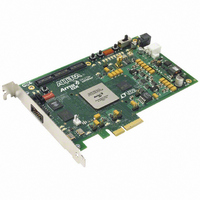
Manufacturer Part Number
DK-DEV-1AGX60N
Description
KIT DEV ARRIA GX 1AGX60N
Manufacturer
Altera
Series
Arria GXr
Type
FPGAr
Datasheet
1.EP1AGX20CF484C6N.pdf
(234 pages)
Specifications of DK-DEV-1AGX60N
Contents
Dev. Board, Quartus® II Web Edition, Reference Designs, Labs, and Complete Documentation
For Use With/related Products
1AGX60N
Lead Free Status / RoHS Status
Lead free / RoHS Compliant
Other names
544-2372
Available stocks
Company
Part Number
Manufacturer
Quantity
Price


2–34
ALM Operating Modes
Arria GX Device Handbook, Volume 1
One ALM contains two programmable registers. Each register has data, clock, clock
enable, synchronous and asynchronous clear, asynchronous load data, and
synchronous and asynchronous load/preset inputs.
Global signals, general-purpose I/O pins, or any internal logic can drive the register's
clock and clear control signals. Either general-purpose I/O pins or internal logic can
drive the clock enable, preset, asynchronous load, and asynchronous load data. The
asynchronous load data input comes from the datae or dataf input of the ALM,
which are the same inputs that can be used for register packing. For combinational
functions, the register is bypassed and the output of the LUT drives directly to the
outputs of the ALM.
Each ALM has two sets of outputs that drive the local, row, and column routing
resources. The LUT, adder, or register output can drive these output drivers
independently (refer to
can drive column, row, or direct link routing connections. One of these ALM outputs
can also drive local interconnect resources. This allows the LUT or adder to drive one
output while the register drives another output. This feature, called register packing,
improves device utilization because the device can use the register and combinational
logic for unrelated functions. Another special packing mode allows the register
output to feed back into the LUT of the same ALM so that the register is packed with
its own fan-out LUT. This feature provides another mechanism for improved fitting.
The ALM can also drive out registered and unregistered versions of the LUT or adder
output.
The Arria GX ALM can operate in one of the following modes:
■
■
■
■
Each mode uses ALM resources differently. Each mode has 11 available inputs to the
ALM (refer to
carry-in from the previous ALM or LAB; the shared arithmetic chain connection from
the previous ALM or LAB; and the register chain connectionare directed to different
destinations to implement the desired logic function. LAB-wide signals provide clock,
asynchronous clear, asynchronous preset/load, synchronous clear, synchronous load,
and clock enable control for the register. These LAB-wide signals are available in all
ALM modes. For more information about LAB-wide control signals, refer to
Control Signals” on page
The Quartus II software and supported third-party synthesis tools, in conjunction
with parameterized functions such as library of parameterized modules (LPM)
functions, automatically choose the appropriate mode for common functions such as
counters, adders, subtractors, and arithmetic functions. If required, you can also
create special-purpose functions that specify which ALM operating mode to use for
optimal performance.
Normal mode
Extended LUT mode
Arithmetic mode
Shared arithmetic mode
Figure
2–28)the eight data inputs from the LAB local interconnect;
Figure
2–30.
2–29). For each set of output drivers, two ALM outputs
© December 2009 Altera Corporation
Chapter 2: Arria GX Architecture
Adaptive Logic Modules
“LAB
Related parts for DK-DEV-1AGX60N
Image
Part Number
Description
Manufacturer
Datasheet
Request
R

Part Number:
Description:
KIT DEV ARRIA II GX FPGA 2AGX125
Manufacturer:
Altera
Datasheet:

Part Number:
Description:
KIT DEV CYCLONE III LS EP3CLS200
Manufacturer:
Altera
Datasheet:

Part Number:
Description:
KIT DEV STRATIX IV FPGA 4SE530
Manufacturer:
Altera
Datasheet:

Part Number:
Description:
KIT DEV FPGA 2AGX260 W/6.375G TX
Manufacturer:
Altera
Datasheet:

Part Number:
Description:
KIT DEV MAX V 5M570Z
Manufacturer:
Altera
Datasheet:

Part Number:
Description:
KIT DEV STRATIX V FPGA 5SGXEA7
Manufacturer:
Altera
Datasheet:

Part Number:
Description:
KIT DEVELOPMENT STRATIX III
Manufacturer:
Altera
Datasheet:

Part Number:
Description:
KIT DEVELOPMENT STRATIX IV
Manufacturer:
Altera
Datasheet:
Part Number:
Description:
KIT STARTER CYCLONE IV GX
Manufacturer:
Altera
Datasheet:
Part Number:
Description:
KIT DEVELOPMENT STRATIX IV
Manufacturer:
Altera
Datasheet:

Part Number:
Description:
CPLD, EP610 Family, ECMOS Process, 300 Gates, 16 Macro Cells, 16 Reg., 16 User I/Os, 5V Supply, 35 Speed Grade, 24DIP
Manufacturer:
Altera Corporation
Datasheet:
Part Number:
Description:
CPLD, EP610 Family, ECMOS Process, 300 Gates, 16 Macro Cells, 16 Reg., 16 User I/Os, 5V Supply, 15 Speed Grade, 24DIP
Manufacturer:
Altera Corporation
Datasheet: