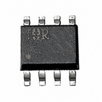
IRF7307 International Rectifier, IRF7307 Datasheet

IRF7307
Specifications of IRF7307
Available stocks
Related parts for IRF7307
IRF7307 Summary of contents
Page 1
... Peak Diode Recovery dv/ Junction and Storage Temperature Range J, STG Thermal Resistance Ratings Parameter R Maximum Junction-to-Ambient P iew Parameter @ 9.1242B IRF7307 ® HEXFET Power MOSFET 8 N- 20V D 2 DSS 0.050 DS(on Max. N-Channel P-Channel 5.7 -4.7 5.2 -4.3 4.1 -3.4 21 -17 2 ...
Page 2
... IRF7307 Electrical Characteristics @ T Parameter V Drain-to-Source Breakdown Voltage (BR)DSS Breakdown Voltage Temp. Coefficient (BR)DSS J R Static Drain-to-Source On-Resistance DS(ON) V Gate Threshold Voltage GS(th) g Forward Transconductance fs I Drain-to-Source Leakage Current DSS I Gate-to-Source Forward Leakage GSS Q Total Gate Charge g Q Gate-to-Source Charge gs Q Gate-to-Drain ("Miller") Charge ...
Page 3
... Drain -to -S ourc e Voltage ( Fig 5. Typical Capacitance Vs. Drain-to-Source Voltage N-Channel Fig 2. Typical Output Characteristics IRF7307 VGS TOP 7.5V 5.0V 4.0V 3.5V 3.0V 2.5V 2.0V B OTTOM 1. .5V 20 µ 0° rain- to- So urc e V oltage ( . unction Tem perature (° Fig 4. Normalized On-Resistance Vs. Temperature ...
Page 4
... IRF7307 150° 25° Sour ce-to-Dr ain Voltage ( V) SD Fig 7. Typical Source-Drain Diode Forward Voltage 6.0 5.0 4.0 3.0 2.0 1.0 0 Case Temperature C Fig 9. Maximum Drain Current Vs. Ambient Temperature Current Regulator Same Type as D.U.T. 50K .2 F 12V . 3mA Current Sampling Resistors Fig 11a ...
Page 5
... Fig 14. Typical Transfer Characteristics Drain- to -So urc e V oltage ( Fig 16. Typical Capacitance Vs. Drain-to-Source Voltage P-Channel Fig 13. Typical Output Characteristics ° IRF7307 VGS TOP - 7. BOTTOM - -1.5V 20µ 150° rain-to-S ourc e Voltage ( - unc tion Tem per ature (° Fig 15. Normalized On-Resistance Vs. Temperature -2. - ...
Page 6
... IRF7307 150° Sour ce-to-Drain V oltage (V) SD Fig 18. Typical Source-Drain Diode Forward Voltage 5.0 4.0 3.0 2.0 1.0 0 Case Temperature C Fig 20. Maximum Drain Current Vs. Ambient Temperature Current Regulator Same Type as D.U.T. 50K .2 F 12V . -3mA Current Sampling Resistors Fig 22a. Gate Charge Test Circuit P-Channel T = 25° ...
Page 7
... D = 0.50 0.20 10 0.10 0.05 0.02 0.01 1 SINGLE PULSE (THERMAL RESPONSE) 0.1 0.0001 0.001 Fig 23. Maximum Effective Transient Thermal Impedance, Junction-to-Ambient N & P-Channel 0.01 0 Rectangular Pulse Duration (sec) 1 IRF7307 Notes: 1. Duty factor Peak thJA 100 ...
Page 8
... IRF7307 D.U Reverse Polarity for P-Channel ** Use P-Channel Driver for P-Channel Measurements Reverse Recovery Current Re-Applied Voltage *** Peak Diode Recovery dv/dt Test Circuit + Circuit Layout Considerations - ** dv/dt controlled controlled by Duty Factor "D" SD D.U.T. - Device Under Test Driver Gate Drive Period P.W. ...
Page 9
... 0.25 (.010 Part Marking Information SO 101 ° 101 IRF7307 INCHES MILLIMETERS DIM MIN MAX MIN MAX A .0532 .0688 1.35 1.75 A1 .0040 .0098 0.10 0.25 B .014 .018 0.36 0.46 C .0075 .0098 0.19 0.25 D .189 .196 4.80 4.98 E .150 .157 3.81 3.99 e .050 BASIC 1 ...
Page 10
... IRF7307 Tape & Reel Information SO-8 Dimensions are shown in millimeters (inches) T ERM INAT DIR ECT IO N 330.00 ( 13.000) MAX . IA- 481 INCLUDES F LANG E DIST DGE 3 D IME MEA SURE D @ HUB TRO LLING DIME NSIO N : MET RIC WORLD HEADQUARTERS: 233 Kansas St., El Segundo, California 90245, Tel: (310) 322 3331 EUROPEAN HEADQUARTERS: Hurst Green, Oxted, Surrey RH8 9BB, UK Tel 1883 732020 IR CANADA: 7321 Victoria Park Ave ...


