LM2650EVAL/NOPB National Semiconductor, LM2650EVAL/NOPB Datasheet
LM2650EVAL/NOPB
Specifications of LM2650EVAL/NOPB
*LM2650EVAL/NOPB
LM2650EVAL


Related parts for LM2650EVAL/NOPB

LM2650EVAL/NOPB Summary of contents
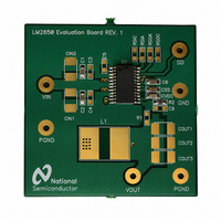
Page 1
... Typical Application Converting a Four-Cell Li Ion Battery to 5V © 2000 National Semiconductor Corporation Features n Ultra high efficiencies (95% possible) n High efficiency over milliamperes load range n Synchronous switching of internal NMOS power FETs n Wide input voltage range (4 ...
Page 2
Connection Diagram Pin Descriptions (Refer to the Block Diagrams) Pins 1, 12 SUB: These pins make electrical contact with the substrate of the die. Ground them. For best thermal performance, ground them to the same large, uninterrupted copper plane as ...
Page 3
... Absolute Maximum Ratings If Military/Aerospace specified devices are required, please contact the National Semiconductor Sales Office/ Distributors for availability and specifications. (All voltages are referenced to the PGND and GND pins.) DC Voltage at PV and Voltage at SD, SLEEP LOGIC and SYNC DC current into SW Junction Temperature ...
Page 4
... See Application Notes on thermal management. The LM2650 actively limits its junction temperature to about 170˚C. Note 3: For detailed information on soldering plastic small-outline packages, refer to the Packaging Databook published by National Semiconductor Corporation. Note 4: ESD is applied using the human-body model, a 100pF capacitor discharged through a 1.5k Note 5: A typical is the center of characterization data taken at T Note 6: All limits are guaranteed ...
Page 5
Typical Performance Characteristics I vs Input Voltage QSD DS012848 Oscillator Frequency Q DS012848-6 R Low-Side vs Junction DS(on) Temperature DS012848-9 Oscillator Frequency vs Adjusting Resistor DS012848- Input Voltage QS DS012848-4 R Low-Side vs Input Voltage DS(on) ...
Page 6
Block Diagrams FIGURE 1. The PWM Circuit with External Components in a Closed Control Loop FIGURE 2. The Hysteretic or Sleep Circuit with External Components in a Closed Control Loop FIGURE 3. The Internal Voltage Regulator and Voltage Reference used ...
Page 7
Operation OVERVIEW The LM2650 uses two step-down conversion modes: fixed-frquency pulse-width modulation (PWM) and hyster- etic. It moves freely and automatically between them, using PWM for moderate to heavy loads and hysteretic for light loads. For clarity, separate block diagrams ...
Page 8
Operation (Continued) The diode D2 is the body diode of Q2. The hysteretic circuit uses rectifier instead of switching synchro- nous rectifier. When the load current drops below the prescribed sleep-in threshold, the LM2650 ...
Page 9
Application Circuits (Continued) TABLE 1. Components for the Typical 90 kHz Application Circuit Input Voltage Applicable Cell Stacks Output Input Capacitor C IN Inductor L1 Output Capacitor C OUT Feedback Resistors R1 and R2 Compensation Components ...
Page 10
Application Circuits (Continued) FIGURE 5. An Efficient, 2% Accurate 5V to 3.3V Converter www.national.com 10 DS012848-20 ...
Page 11
... NATIONAL’S PRODUCTS ARE NOT AUTHORIZED FOR USE AS CRITICAL COMPONENTS IN LIFE SUPPORT DEVICES OR SYSTEMS WITHOUT THE EXPRESS WRITTEN APPROVAL OF THE PRESIDENT AND GENERAL COUNSEL OF NATIONAL SEMICONDUCTOR CORPORATION. As used herein: 1. Life support devices or systems are devices or systems which, (a) are intended for surgical implant ...