SD12CT1G ON Semiconductor, SD12CT1G Datasheet - Page 2
SD12CT1G
Manufacturer Part Number
SD12CT1G
Description
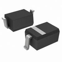
TVS ZENER 350W 12V ESD SOD323
Manufacturer
ON Semiconductor
Datasheet
1.SD12CT1G.pdf
(3 pages)
Specifications of SD12CT1G
Voltage - Reverse Standoff (typ)
12V
Voltage - Breakdown
13.3V
Power (watts)
350W
Polarization
Bidirectional
Mounting Type
Surface Mount
Package / Case
SC-76, SOD-323, UMD2
Polarity
Bidirectional
Clamping Voltage
19 V
Operating Voltage
12 V
Breakdown Voltage
13.3 V
Termination Style
SMD/SMT
Peak Surge Current
15 A
Peak Pulse Power Dissipation
350 W
Capacitance
64 pF
Maximum Operating Temperature
+ 150 C
Minimum Operating Temperature
- 65 C
Dimensions
1.25 mm W x 1.7 mm L
Lead Free Status / RoHS Status
Lead free / RoHS Compliant
Other names
SD12CT1GOSTR
Available stocks
Company
Part Number
Manufacturer
Quantity
Price
Company:

Part Number:
SD12CT1G
Manufacturer:
ON Semiconductor
Quantity:
321 171
Company:
Part Number:
SD12CT1G
Manufacturer:
ON Semiconductor
Quantity:
10
Company:
Part Number:
SD12CT1G
Manufacturer:
ON
Quantity:
30 000
Part Number:
SD12CT1G
Manufacturer:
ON/安森美
Quantity:
20 000


Stresses exceeding Maximum Ratings may damage the device. Maximum Ratings are stress ratings only. Functional operation above the
Recommended Operating Conditions is not implied. Extended exposure to stresses above the Recommended Operating Conditions may affect
device reliability.
1. Minimum Solder Footprint.
ELECTRICAL CHARACTERISTICS
(T
MAXIMUM RATINGS
ELECTRICAL CHARACTERISTICS
2. TVS devices are normally selected according to the working peak reverse voltage (V
3. V
Peak Power Dissipation @ 20 ms @ T
IEC 61000−4−2 (ESD)
IEC 61000−4−4 (EFT)
Total Device Dissipation FR−5 Board,
Thermal Resistance from Junction−to−Ambient
Junction and Storage Temperature Range
Lead Solder Temperature − Maximum (10 Second Duration)
Reverse Working Voltage
Breakdown Voltage
Reverse Leakage Current
Clamping Voltage
Additional Clamping Voltage
Maximum Peak Pulse Current
Capacitance
Symbol
A
V
QV
V
= 25°C unless otherwise noted)
I
RWM
V
or continuous peak operating voltage level.
I
(Note 1) @ T
Derate above 25°C
PP
I
BR
R
T
C
BR
BR
is measured at pulse test current I
Maximum Reverse Peak Pulse Current
Clamping Voltage @ I
Working Peak Reverse Voltage
Maximum Reverse Leakage Current @ V
Breakdown Voltage @ I
Test Current
Maximum Temperature Variation of V
A
= 25°C
Parameter
Parameter
PP
T
Rating
L
≤ 25°C
(T
T
.
J
= 25°C, unless otherwise specified)
BR
I
I
PP
PP
RWM
= 15 A, (8 x 20 msec Waveform)
= 5 A, (8 x 20 msec Waveform)
http://onsemi.com
8 x 20 msec Waveform
V
V
I
T
R
R
SD12CT1
= 1 mA, (Note 3)
= 12 V, f = 1 MHz
V
= 0 V, f = 1 MHz
Conditions
RWM
(Note 2)
2
= 12 V
Contact
Air
V
RWM
C
Symbol
T
V
R
J
P
), which should be equal or greater than the DC
BR
P
Symbol
, T
T
qJA
V
pk
D
L
Bi−Directional TVS
V
RWM
I
stg
V
I
C
PP
V
BR
R
C
j
RWM
I
PP
I
I
R
T
13.3
Min
I
I
I
I
−65 to +150
R
T
PP
Value
V
350
±30
±30
200
635
260
1.5
40
RWM
Typ
64
36
V
BR
V
C
Max
1.0
12
19
24
15
V
mW/°C
°C/W
Unit
mW
kV
°C
°C
W
A
Unit
mA
pF
V
V
V
A
Related parts for SD12CT1G
Image
Part Number
Description
Manufacturer
Datasheet
Request
R

Part Number:
Description:
ON Semiconductor [VOLTAGE REGULATOR]
Manufacturer:
ON Semiconductor
Datasheet:
Part Number:
Description:
357-036-542-201 CARDEDGE 36POS DL .156 BLK LOPRO
Manufacturer:
ON Semiconductor
Datasheet:
Part Number:
Description:
357-036-542-201 CARDEDGE 36POS DL .156 BLK LOPRO
Manufacturer:
ON Semiconductor
Datasheet:
Part Number:
Description:
357-036-542-201 CARDEDGE 36POS DL .156 BLK LOPRO
Manufacturer:
ON Semiconductor
Datasheet:
Part Number:
Description:
357-036-542-201 CARDEDGE 36POS DL .156 BLK LOPRO
Manufacturer:
ON Semiconductor
Datasheet:
Part Number:
Description:
357-036-542-201 CARDEDGE 36POS DL .156 BLK LOPRO
Manufacturer:
ON Semiconductor
Datasheet:
Part Number:
Description:
357-036-542-201 CARDEDGE 36POS DL .156 BLK LOPRO
Manufacturer:
ON Semiconductor
Datasheet:
Part Number:
Description:
357-036-542-201 CARDEDGE 36POS DL .156 BLK LOPRO
Manufacturer:
ON Semiconductor
Datasheet:
Part Number:
Description:
357-036-542-201 CARDEDGE 36POS DL .156 BLK LOPRO
Manufacturer:
ON Semiconductor
Datasheet:
Part Number:
Description:
357-036-542-201 CARDEDGE 36POS DL .156 BLK LOPRO
Manufacturer:
ON Semiconductor
Datasheet:
Part Number:
Description:
357-036-542-201 CARDEDGE 36POS DL .156 BLK LOPRO
Manufacturer:
ON Semiconductor
Datasheet:
Part Number:
Description:
Manufacturer:
ON Semiconductor
Datasheet:
Part Number:
Description:
Manufacturer:
ON Semiconductor
Datasheet:
Part Number:
Description:
Manufacturer:
ON Semiconductor
Datasheet: