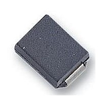
SACB7.0 Littelfuse Inc, SACB7.0 Datasheet - Page 2

SACB7.0
Manufacturer Part Number
SACB7.0
Description
DIODE TVS 7V 500W UNI SMD
Manufacturer
Littelfuse Inc
Series
SACBr
Datasheet
1.SACB12.pdf
(4 pages)
Specifications of SACB7.0
Voltage - Reverse Standoff (typ)
7V
Voltage - Breakdown
8.33V
Power (watts)
500W
Polarization
Unidirectional
Mounting Type
Surface Mount
Package / Case
DO-214AA, SMB
Reverse Stand-off Voltage Vrwm
7V
Breakdown Voltage Range
8.33V
Clamping Voltage Vc Max
12.6V
Diode Configuration
Unidirectional
Peak Pulse Current Ippm
38A
Diode Case Style
DO-214AA
No. Of Pins
2
Polarity
Unidirectional
Channels
1 Channel
Clamping Voltage
12.6 V
Operating Voltage
7 V
Breakdown Voltage
8.33 V
Termination Style
SMD/SMT
Peak Surge Current
38 A
Peak Pulse Power Dissipation
500 W
Capacitance
45 pF
Maximum Operating Temperature
+ 150 C
Minimum Operating Temperature
- 65 C
Dimensions
3.94 mm W x 4.57 mm L x 2.44 mm H
Lead Free Status / RoHS Status
Lead free / RoHS Compliant
Lead Free Status / RoHS Status
Lead free / RoHS Compliant, Lead free / RoHS Compliant
Available stocks
Company
Part Number
Manufacturer
Quantity
Price
Part Number:
SACB7.0
Manufacturer:
VISHAY/威世
Quantity:
20 000
SACB Series
Number
SACB5.0
SACB6.0
SACB8.0
SACB8.5
SACB7 .0
SACB18
SACB22
SACB26
SACB30
SACB36
SACB45
SACB50
Electrical Characteristics
SACB10
SACB12
SACB15
Ratings and Characteristic Curves
Ratings and Characteristic Curves
Figure 1 - Peak Pulse Power Rating Curve
Figure 3 - Pulse Waveform
Part
100
30
Marking
0.1
10
1
0.1s
150
100
Code
SKM
SLM
SME
SMK
SMP
SMV
SMZ
SKG
50
SKE
SKR
SKT
SKX
SLE
SLX
SLT
0
P
PK
P
P
PK
".5"
PK
Current Waveforms
0
td
td
td
(Note1) V
1.0s
Stand-Off
t d
Voltage
Half Sine
Square
td=7tp
t r =10μsec
22.0
26.0
30.0
36.0
45.0
50.0
10.0
12.0
15.0
18.0
Transient Voltage Suppression Diodes
Surface Mount – 500W > SACB series
(V)
5.0
6.0
8.0
8.5
7 .0
Exponential
Impulse
Decay
Peak Value
I PPM
t
1.0
d
- Pulse Width (sec.)
10s
R
Breakdown
t-Time (ms)
Minimum
Voltage at
Half Value
I PPM
I
T
=1.0MA
V
Waveform shown in Fig. 3
Non-repetitive Pulse
13.30
16.70
20.00
24.40
28.90
33.30
40.00
50.00
55.50
11.10
T
8.33
8.89
9.44
7 .60
7 .90
BR
A
2.0
=25°C
(V)
100s
( )
I PPM
2
10/1000μsec. Waveform
as defined by R.E.A
T J =25°C
Pulse Width(td) is defined
as the point where the peak
current decays to 50% of I PPM
(T
(T
A
A
Maximum
=25°C unless otherwise noted
= 25°C unless otherwise noted)
Leakage
Reverse
1.0ms
at V
3.0
(μA)
300
300
300
100
50
5
5
5
5
5
5
5
5
5
5
R
I
R
10ms
Maximum
Clamping
Voltage at
I
4.0
PP
V
10.0
12.6
13.4
14.0
16.3
19.0
23.6
28.8
35.4
42.3
48.6
60.0
88.0
=5.0A
11.2
77 .0
C
(V)
Revision: January 09, 2009
Maximum
per (Fig.3)
Current
20
Pulse
I
Peak
PP
44.0
41.0
38.0
36.0
34.0
29.0
25.0
20.0
15.0
14.0
10.0
11.1
8.6
6.8
5.8
(A)
Figure 2 - Pulse Derating Curve
Figure 4 - AC Line Protection Application
Capacitance
0 Volts (pF)
Maximum
Junction
45
45
45
45
45
45
45
45
45
45
45
45
45
45
45
at
Please refer to http://www.Littelfuse.com/series/SACB.html for current information.
100
75
50
25
0
0
Application Note: Device must be used with two
units in parallel, opposite in polarity as shown in
circuit for AC signal line protection.
Working
Blocking
Voltage
Inverse
V
WIB
150
150
25
75
75
75
75
75
75
75
75
75
75
75
75
75
Low Capacitance
(V)
T
(Single Pulse)
L
Peak Power
- Lead Temperature (ºC)
50
Current at
Blocking
V
Leakage
Inverse
WIB
Specifications are subject to change without notice.
(mA)
1.0
1.0
1.0
1.0
1.0
1.0
1.0
1.0
1.0
1.0
1.0
1.0
1.0
1.0
1.0
@ I
75
IB
Peak Inverse
Voltage V
100
Average Power
Blocking
200
200
100
100
100
100
100
100
100
100
100
100
100
100
100
(V)
125
PIB
©2009 Littelfuse, Inc.
Recognition
150
UL
X
X
X
X
X
X
X
X
X
X
X
X
X
X
X


