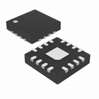
MAX3205EETE+ Maxim Integrated Products, MAX3205EETE+ Datasheet - Page 7

MAX3205EETE+
Manufacturer Part Number
MAX3205EETE+
Description
IC ESD PROT DIFF 16-TQFN
Manufacturer
Maxim Integrated Products
Datasheet
1.MAX3208EAUB.pdf
(9 pages)
Specifications of MAX3205EETE+
Power (watts)
1.66W
Polarization
6 Channel Array - Unidirectional
Mounting Type
Surface Mount
Package / Case
16-TQFN Exposed Pad
Lead Free Status / RoHS Status
Lead free / RoHS Compliant
Voltage - Breakdown
-
Voltage - Reverse Standoff (typ)
-
Proper circuit-board layout is critical to suppress ESD-
induced line transients (See Figure 6). The MAX3205E/
MAX3207E/MAX3208E clamp to 100V; however, with
improper layout, the voltage spike at the device can be
much higher. A lead inductance of 10nH with a 45A
current spike results in an additional 450V spike on the
protected line. It is essential that the layout of the PC
board follows these guidelines:
1) Minimize trace length between the connector or
2) Use separate planes for power and ground to reduce
3) Ensure short low-inductance ESD transient return
4) Minimize conductive power and ground loops.
5) Do not place critical signals near the edge of the PC
Figure 6. Layout Considerations
input terminal, I/O_, and the protected signal line.
parasitic inductance and to reduce the impedance to
the power rails for shunted ESD current.
paths to GND and V
board.
NEGATIVE ESD-
CURRENT
PULSE
PATH TO
GROUND
GND
V
PROTECTED LINE
CC
L1
_______________________________________________________________________________________
D1
D2
Layout Recommendations
CC
I/O_
.
L2
L3
Dual, Quad, and Hex High-Speed
V
C
Differential ESD-Protection ICs
PROTECTED
CIRCUIT
6) Bypass V
7) Bypass the supply of the protected device to GND
For the latest application details on WLP construction,
dimensions, tape carrier information, printed circuit
board techniques, bump-pad layout, and recommend-
ed reflow temperature profile, as well as the latest infor-
mation on reliability testing results, refer to Application
Note 1891: Wafer-Level Packaging (WLP) and Its
Applications .
PROCESS: BiCMOS
0.1μF
tor as close to V
with a low-ESR ceramic capacitor as close to the
supply pin as possible.
V
CC
WLP Applications Information
I/0 LINE
CC
Typical Operating Circuit
I/0_
MAX3205E
MAX3207E
MAX3208E
to GND with a low-ESR ceramic capaci-
CC
as possible.
Chip Information
0.1μF
V
CC
I/0
PROTECTED
CIRCUIT
7


