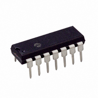
PIC16F526-E/P Microchip Technology, PIC16F526-E/P Datasheet - Page 69

PIC16F526-E/P
Manufacturer Part Number
PIC16F526-E/P
Description
IC PIC MCU FLASH 1KX12 14DIP
Manufacturer
Microchip Technology
Series
PIC® 16Fr
Specifications of PIC16F526-E/P
Core Size
8-Bit
Program Memory Size
1.5KB (1K x 12)
Core Processor
PIC
Speed
20MHz
Peripherals
POR, WDT
Number Of I /o
11
Program Memory Type
FLASH
Ram Size
67 x 8
Voltage - Supply (vcc/vdd)
2 V ~ 5.5 V
Data Converters
A/D 3x8b
Oscillator Type
Internal
Operating Temperature
-40°C ~ 125°C
Package / Case
14-DIP (0.300", 7.62mm)
Controller Family/series
PIC16F
No. Of I/o's
12
Ram Memory Size
67Byte
Cpu Speed
20MHz
No. Of Timers
1
Digital Ic Case Style
DIP
Processor Series
PIC16F
Core
PIC
Data Bus Width
8 bit
Data Ram Size
67 B
Maximum Clock Frequency
20 MHz
Number Of Programmable I/os
12
Number Of Timers
1
Maximum Operating Temperature
+ 125 C
Mounting Style
Through Hole
3rd Party Development Tools
52715-96, 52716-328, 52717-734
Development Tools By Supplier
PG164130, DV164035, DV244005, DV164005, PG164120, ICE2000
Minimum Operating Temperature
- 40 C
On-chip Adc
8 bit, 3 Channel
Lead Free Status / RoHS Status
Lead free / RoHS Compliant
For Use With
AC162096 - HEADER MPLAB ICD2 PIC16F526 8/14
Eeprom Size
-
Connectivity
-
Lead Free Status / Rohs Status
Details
11.0
The Comparator Voltage Reference module also
allows the selection of an internally generated voltage
reference for one of the C2 comparator inputs. The
VRCON register (Register 11-1) controls the Voltage
Reference module shown in Figure 11-1.
11.1
The voltage reference can output 32 voltage levels; 16
in a high range and 16 in a low range.
Equation 11-1 determines the output voltages:
EQUATION 11-1:
REGISTER 11-1:
2010 Microchip Technology Inc.
bit 7
Legend:
R = Readable bit
-n = Value at POR
bit 7
bit 6
bit 5
bit 4
bit 3-0
VRR = 0 (high range):
VRR = 1 (low range): CV
Note 1: When this bit is set, the TRIS for the CV
R/W-0
VREN
CV
COMPARATOR VOLTAGE
REFERENCE MODULE
Configuring The Voltage
Reference
REF
CV
= (V
REF
VREN: CV
1 = CV
0 = CV
VROE: CV
1 = CV
0 = CV
VRR: CV
1 = Low range
0 = High range
Unimplemented: Read as ‘0’
VR<3:0> CV
When V
When V
DD
pin.
R/W-0
VROE
/4) + (VR<3:0> x V
VRCON: VOLTAGE REFERENCE CONTROL REGISTER
REF
REF
REF
REF
RR
RR
REF
REF
REF
REF
= 1: CV
= 0: CV
is powered on
is powered down, no current is drawn
output is enabled
output is disabled
= (VR<3:0>/24) x V
REF
Range Selection bit
W = Writable bit
‘1’ = Bit is set
Enable bit
Output Enable bit
Value Selection bit
R/W-0
VRR
REF
REF
= (VR<3:0>/24)*V
= V
DD
/32)
DD
/4+(VR<3:0>/32)*V
DD
(1)
U-0
—
REF
DD
pin is overridden and the analog voltage is placed on the
U = Unimplemented bit, read as ‘0’
‘0’ = Bit is cleared
R/W-0
11.2
The full range of V
construction of the module. The transistors on the top
and bottom of the resistor ladder network (Figure 11-1)
keep CV
exception is when the module is disabled by clearing
the VREN bit of the VRCON register. When disabled,
the reference voltage is V
and the VRR bit of the VRCON register is set. This
allows the comparator to detect a zero-crossing and
not consume the CV
The voltage reference is V
the CV
The tested absolute accuracy of the comparator
voltage reference can be found in Section 14.0 “Elec-
trical Characteristics”.
VR3
DD
REF
Voltage Reference Accuracy/Error
REF
output changes with fluctuations in V
R/W-0
from approaching V
VR2
SS
REF
to V
module current.
DD
x = Bit is unknown
PIC16F526
SS
DD
cannot be realized due to
when VR<3:0> is ‘0000’
R/W-0
VR1
derived and, therefore,
SS
DS41326E-page 69
or V
R/W-0
VR0
DD
. The
bit 0
DD
.


