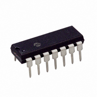
PIC16F616-I/P Microchip Technology, PIC16F616-I/P Datasheet - Page 8

PIC16F616-I/P
Manufacturer Part Number
PIC16F616-I/P
Description
IC PIC MCU FLASH 2KX14 14DIP
Manufacturer
Microchip Technology
Series
PIC® 16Fr
Datasheets
1.PIC12F609T-ISN.pdf
(26 pages)
2.PIC16F616T-ISL.pdf
(4 pages)
3.PIC16F616T-ISL.pdf
(214 pages)
4.PIC16F616T-ISL.pdf
(8 pages)
5.PIC16F616-ESL.pdf
(180 pages)
Specifications of PIC16F616-I/P
Core Size
8-Bit
Program Memory Size
3.5KB (2K x 14)
Peripherals
Brown-out Detect/Reset, POR, PWM, WDT
Core Processor
PIC
Speed
20MHz
Number Of I /o
11
Program Memory Type
FLASH
Ram Size
128 x 8
Voltage - Supply (vcc/vdd)
2 V ~ 5.5 V
Data Converters
A/D 8x10b
Oscillator Type
Internal
Operating Temperature
-40°C ~ 85°C
Package / Case
14-DIP (0.300", 7.62mm)
Controller Family/series
PIC16F
No. Of I/o's
12
Ram Memory Size
128Byte
Cpu Speed
20MHz
No. Of Timers
3
Package
14PDIP
Device Core
PIC
Family Name
PIC16
Maximum Speed
20 MHz
Operating Supply Voltage
2.5|3.3|5 V
Data Bus Width
8 Bit
Number Of Programmable I/os
11
On-chip Adc
8-chx10-bit
Number Of Timers
3
Processor Series
PIC16F
Core
PIC
Data Ram Size
128 B
Maximum Clock Frequency
20 MHz
Maximum Operating Temperature
+ 85 C
Mounting Style
Through Hole
3rd Party Development Tools
52715-96, 52716-328, 52717-734
Development Tools By Supplier
PG164130, DV164035, DV244005, DV164005, PG164120, ICE2000
Minimum Operating Temperature
- 40 C
Lead Free Status / RoHS Status
Lead free / RoHS Compliant
For Use With
MCP1631RD-DCPC1 - REF DES BATT CHARG OR LED DRIVERAC162083 - HEADER MPLAB ICD2 PIC16F616 8/14AC124001 - MODULE SKT PROMATEII 8DIP/SOIC
Eeprom Size
-
Connectivity
-
Lead Free Status / Rohs Status
Details
PIC12F609/12F615/12F617/16F610/16F616 AND PIC12HV609/12HV615/16HV610/16HV616
4.1.3
The PIC12F609/12F615/12F617/16F610/16F616 and
PIC12HV609/12HV615/16HV610/16HV616 devices will
erase different memory locations depending on the PC
and CP. The following sequences can be used to erase
noted memory locations. To erase the program memory
and Configuration Word (0x2007), the following sequence
must be performed. Note the Calibration Word (0x2008)
and User ID (0x2000-0x2003) will not be erased.
1.
2.
To erase the User ID (0x2000-0x2003), Configuration
Word (0x2007) and program memory, use the following
sequence. Note that the Calibration Word (0x2008) will
not be erased.
1.
2.
3.
DS41396A-page 8
Do a Bulk Erase Program Memory command.
Wait T
Perform Load Configuration with dummy data to
point the PC to 0x2000.
Perform a Bulk Erase Program Memory
command.
Wait T
ERA
ERA
ERASE ALGORITHMS
to complete erase.
to complete erase.
4.1.4
The ICSPCLK pin is used as a clock input and the
ICSPDAT pin is used for entering command bits and
data input/output during serial operation. To input a
command, ICSPCLK is cycled six times. Each
command bit is latched on the falling edge of the clock
with the LSb of the command being input first. The data
input onto the ICSPDAT pin is required to have a mini-
mum setup and hold time (see Table 7-1), with respect
to the falling edge of the clock. Commands that have
data associated with them (Read and Load) are
specified to have a minimum delay of 1 s between the
command and the data. After this delay, the clock pin is
cycled 16 times with the first cycle being a Start bit and
the last cycle being a Stop bit.
During a read operation, the LSb will be transmitted
onto the ICSPDAT pin on the rising edge of the second
cycle. For a load operation, the LSb will be latched on
the falling edge of the second cycle. A minimum 1 s
delay
commands,
command, which requires a 100 s (T
All commands and data words are transmitted LSb first.
Data is transmitted on the rising edge and latched on
the falling edge of the ICSPCLK. To allow for decoding
of commands and reversal of data pin configuration, a
time separation of at least 1 s (T
between a command and a data word.
The commands that are available are described in
Table 4-1.
is
SERIAL PROGRAM/VERIFY
OPERATION
also
except
specified
for
2009 Microchip Technology Inc.
the
between
End
DLY
DIS
1) is required
Programming
).
consecutive


