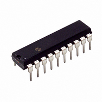
PIC16F677-I/P Microchip Technology, PIC16F677-I/P Datasheet - Page 68

PIC16F677-I/P
Manufacturer Part Number
PIC16F677-I/P
Description
IC PIC MCU FLASH 2KX14 20DIP
Manufacturer
Microchip Technology
Series
PIC® 16Fr
Datasheets
1.PIC16F616T-ISL.pdf
(8 pages)
2.PIC16F690DM-PCTLHS.pdf
(306 pages)
3.PIC16F677-IP.pdf
(2 pages)
4.PIC16F677-IP.pdf
(16 pages)
5.PIC16F677-ISO.pdf
(294 pages)
Specifications of PIC16F677-I/P
Program Memory Type
FLASH
Program Memory Size
3.5KB (2K x 14)
Package / Case
20-DIP (0.300", 7.62mm)
Mfg Application Notes
Intro to Capacitive Sensing Appl Notes Layout and Physical Design Appl Note
Core Processor
PIC
Core Size
8-Bit
Speed
20MHz
Connectivity
I²C, SPI
Peripherals
Brown-out Detect/Reset, POR, WDT
Number Of I /o
18
Eeprom Size
256 x 8
Ram Size
128 x 8
Voltage - Supply (vcc/vdd)
2 V ~ 5.5 V
Data Converters
A/D 12x10b
Oscillator Type
Internal
Operating Temperature
-40°C ~ 85°C
Processor Series
PIC16F
Core
PIC
Data Bus Width
8 bit
Data Ram Size
128 B
Interface Type
SSP
Maximum Clock Frequency
20 MHz
Number Of Programmable I/os
17
Number Of Timers
2
Operating Supply Voltage
2 V to 5.5 V
Maximum Operating Temperature
+ 85 C
Mounting Style
Through Hole
3rd Party Development Tools
52715-96, 52716-328, 52717-734
Development Tools By Supplier
PG164130, DV164035, DV244005, DV164005, PG164120, ICE2000, DM163014, DM164120-4
Minimum Operating Temperature
- 40 C
On-chip Adc
12-ch x 10-bit
Lead Free Status / RoHS Status
Lead free / RoHS Compliant
For Use With
AC162061 - HEADER INTRFC MPLAB ICD2 20PINACICE0203 - MPLABICE 20P 300 MIL ADAPTER
Lead Free Status / Rohs Status
Lead free / RoHS Compliant
Available stocks
Company
Part Number
Manufacturer
Quantity
Price
Company:
Part Number:
PIC16F677-I/P
Manufacturer:
MICROCHIP
Quantity:
2 000
- PIC16F616T-ISL PDF datasheet
- PIC16F690DM-PCTLHS PDF datasheet #2
- PIC16F677-IP PDF datasheet #3
- PIC16F677-IP PDF datasheet #4
- PIC16F677-ISO PDF datasheet #5
- Current page: 68 of 306
- Download datasheet (6Mb)
PIC16F631/677/685/687/689/690
4.2.5.4
Figure 4-4 shows the diagram for this pin. The
RA3/MCLR/V
of the following:
• a general purpose input
• as Master Clear Reset with weak pull-up
FIGURE 4-4:
DS41262E-page 66
Data Bus
PORTA
IOCA
IOCA
TRISA
WR
Interrupt-on-
RD
RD
RD
Change
D
CK
RA3/MCLR/V
PP
Q
Q
pin is configurable to function as one
Reset
MCLRE
BLOCK DIAGRAM OF RA3
V
SS
PP
RD PORTA
MCLRE
Q
Q
MCLRE
EN
EN
D
D
V
DD
Weak
V
SS
Q3
Input
Pin
4.2.5.5
Figure 4-5 shows the diagram for this pin. The
RA4/AN3/T1G/OSC2/CLKOUT pin is configurable to
function as one of the following:
• a general purpose I/O
• an analog input for the ADC (except PIC16F631)
• a Timer1 gate input
• a crystal/resonator connection
• a clock output
FIGURE 4-5:
Data Bus
PORTA
PORTA
WPUA
WPUA
TRISA
TRISA
IOCA
IOCA
Note 1: CLK modes are XT, HS, LP, LPTMR1 and CLKOUT
WR
WR
WR
WR
RD
RD
RD
RD
Interrupt-on-
Change
2: With CLKOUT option.
3: ANSEL determines Analog Input mode.
4: Not implemented on PIC16F631.
Enable.
D
D
D
D
To T1G
To A/D Converter
CK
CK
CK
CK
RA4/AN3/T1G/OSC2/CLKOUT
Q
Q
Q
Q
Q
Q
Q
Q
Input Mode
BLOCK DIAGRAM OF RA4
Analog
© 2008 Microchip Technology Inc.
OSC1
(4)
F
OSC
INTOSC/
RC/EC
CLKOUT
CLKOUT
(3)
Enable
Enable
Input Mode
/4
RABPU
RD PORTA
CLKOUT
Analog
Enable
Oscillator
Circuit
Modes
Q
Q
1
0
(2)
CLK
EN
EN
(1)
D
D
V
DD
Weak
V
V
DD
SS
Q3
I/O Pin
Related parts for PIC16F677-I/P
Image
Part Number
Description
Manufacturer
Datasheet
Request
R

Part Number:
Description:
3.5KB Flash, 128B RAM, 18 I/O, CLC, CWG, DDS, 10-bit ADC 20 QFN 4x4mm TUBE
Manufacturer:
Microchip Technology
Datasheet:

Part Number:
Description:
3.5KB Flash, 128B RAM, 18 I/O, CLC, CWG, DDS, 10-bit ADC 20 PDIP .300in TUBE
Manufacturer:
Microchip Technology
Datasheet:

Part Number:
Description:
3.5KB Flash, 128B RAM, 18 I/O, CLC, CWG, DDS, 10-bit ADC 20 SOIC .300in TUBE
Manufacturer:
Microchip Technology
Datasheet:

Part Number:
Description:
3.5KB Flash, 128B RAM, 18 I/O, CLC, CWG, DDS, 10-bit ADC 20 SSOP .209in TUBE
Manufacturer:
Microchip Technology
Datasheet:

Part Number:
Description:
3.5KB Flash, 128B RAM, 18 I/O, CLC, CWG, DDS, 10-bit ADC 20 QFN 4x4mm TUBE
Manufacturer:
Microchip Technology
Datasheet:

Part Number:
Description:
3.5KB Flash, 128B RAM, 18 I/O, CLC, CWG, DDS, 10-bit ADC 20 PDIP .300in TUBE
Manufacturer:
Microchip Technology
Datasheet:

Part Number:
Description:
3.5KB Flash, 128B RAM, 18 I/O, CLC, CWG, DDS, 10-bit ADC 20 SOIC .300in TUBE
Manufacturer:
Microchip Technology
Datasheet:

Part Number:
Description:
3.5KB Flash, 128B RAM, 18 I/O, CLC, CWG, DDS, 10-bit ADC 20 SSOP .209in TUBE
Manufacturer:
Microchip Technology
Datasheet:

Part Number:
Description:
3.5KB Flash, 128B RAM, 18 I/O, CLC, CWG, DDS, 10-bit ADC 20 QFN 4x4mm T/R
Manufacturer:
Microchip Technology
Datasheet:

Part Number:
Description:
3.5KB Flash, 128B RAM, 18 I/O, CLC, CWG, DDS, 10-bit ADC 20 SOIC .300in T/R
Manufacturer:
Microchip Technology
Datasheet:

Part Number:
Description:
3.5KB Flash, 128B RAM, 18 I/O, CLC, CWG, DDS, 10-bit ADC 20 SSOP .209in T/R
Manufacturer:
Microchip Technology
Datasheet:

Part Number:
Description:
3.5KB Flash, 128B RAM, 18 I/O, CLC, CWG, DDS, 10-bit ADC 20 QFN 4x4mm TUBE
Manufacturer:
Microchip Technology
Datasheet:

Part Number:
Description:
3.5KB Flash, 128B RAM, 18 I/O, CLC, CWG, DDS, 10-bit ADC 20 PDIP .300in TUBE
Manufacturer:
Microchip Technology
Datasheet:

Part Number:
Description:
3.5KB Flash, 128B RAM, 18 I/O, CLC, CWG, DDS, 10-bit ADC 20 SOIC .300in TUBE
Manufacturer:
Microchip Technology
Datasheet:

Part Number:
Description:
3.5KB Flash, 128B RAM, 18 I/O, CLC, CWG, DDS, 10-bit ADC 20 SSOP .209in TUBE
Manufacturer:
Microchip Technology
Datasheet:


