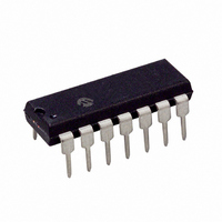
PIC16F676-I/P Microchip Technology, PIC16F676-I/P Datasheet - Page 45

PIC16F676-I/P
Manufacturer Part Number
PIC16F676-I/P
Description
IC MCU FLASH 1K W/AD 14-DIP
Manufacturer
Microchip Technology
Series
PIC® 16Fr
Datasheets
1.PIC16F616T-ISL.pdf
(8 pages)
2.PIC12F629T-ISN.pdf
(24 pages)
3.PIC16F630-ISL.pdf
(132 pages)
4.PIC16F630-ISL.pdf
(2 pages)
5.PIC16F630-ISL.pdf
(10 pages)
6.PIC16F676-EP.pdf
(132 pages)
Specifications of PIC16F676-I/P
Program Memory Type
FLASH
Program Memory Size
1.75KB (1K x 14)
Package / Case
14-DIP (0.300", 7.62mm)
Core Processor
PIC
Core Size
8-Bit
Speed
20MHz
Peripherals
Brown-out Detect/Reset, POR, WDT
Number Of I /o
12
Eeprom Size
128 x 8
Ram Size
64 x 8
Voltage - Supply (vcc/vdd)
2 V ~ 5.5 V
Data Converters
A/D 8x10b
Oscillator Type
Internal
Operating Temperature
-40°C ~ 85°C
Processor Series
PIC16F
Core
PIC
Data Bus Width
8 bit
Data Ram Size
64 B
Interface Type
RS- 232/USB
Maximum Clock Frequency
20 MHz
Number Of Programmable I/os
12
Number Of Timers
2
Operating Supply Voltage
2 V to 5.5 V
Maximum Operating Temperature
+ 85 C
Mounting Style
Through Hole
3rd Party Development Tools
52715-96, 52716-328, 52717-734
Development Tools By Supplier
PG164130, DV164035, DV244005, DV164005, PG164120, ICE2000, DM163014, DM164120-4
Minimum Operating Temperature
- 40 C
On-chip Adc
8-ch x 10-bit
Data Rom Size
128 B
Height
3.3 mm
Length
19.05 mm
Supply Voltage (max)
5.5 V
Supply Voltage (min)
2 V
Width
6.35 mm
Lead Free Status / RoHS Status
Lead free / RoHS Compliant
For Use With
DM163029 - BOARD PICDEM FOR MECHATRONICSAC124001 - MODULE SKT PROMATEII 8DIP/SOIC
Connectivity
-
Lead Free Status / Rohs Status
Lead free / RoHS Compliant
Available stocks
Company
Part Number
Manufacturer
Quantity
Price
Company:
Part Number:
PIC16F676-I/P
Manufacturer:
RENESAS
Quantity:
5 600
Part Number:
PIC16F676-I/P
Manufacturer:
MICROCHIP/微芯
Quantity:
20 000
7.0
The Analog-to-Digital Converter (ADC) allows conver-
sion of an analog input signal to a 10-bit binary repre-
sentation of that signal. The PIC16F676 has eight
analog inputs, multiplexed into one sample and hold
FIGURE 7-1:
7.1
There are three registers available to control the
functionality of the A/D module:
1.
2.
3.
7.1.1
The ANS7:ANS0 bits (ANSEL<7:0>) and the TRISA
bits control the operation of the A/D port pins. Set the
corresponding TRISA bits to set the pin output driver to
its high-impedance state. Likewise, set the correspond-
ing ANS bit to disable the digital input buffer.
7.1.2
There are eight analog channels on the PIC16F676,
AN0
(ADCON0<4:2>) control which channel is connected to
the sample and hold circuit.
2010 Microchip Technology Inc.
Note:
ADCON0 (Register 7-1)
ADCON1 (Register 7-2)
ANSEL (Register 7-3)
through
ANALOG-TO-DIGITAL
CONVERTER (A/D) MODULE
(PIC16F676 ONLY)
A/D Configuration and Operation
Analog voltages on any pin that is defined
as a digital input may cause the input
buffer to conduct excess current.
ANALOG PORT PINS
CHANNEL SELECTION
RA1/AN1/V
AN7.
A/D BLOCK DIAGRAM
RC0/AN4
RA4/AN3
RC1/AN5
RC2/AN6
RC3/AN7
RA0/AN0
RA2/AN2
The
REF
CHS2:CHS0
CHS2:CHS0
V
REF
bits
V
DD
GO/DONE
VCFG = 0
VCFG = 1
ADON
circuit. The output of the sample and hold is connected
to the input of the converter. The converter generates a
binary result via successive approximation and stores
the result in a 10-bit register. The voltage reference
used in the conversion is software selectable to either
V
shows the block diagram of the A/D on the PIC16F676.
7.1.3
There are two options for the voltage reference to the
A/D converter: either V
applied to V
controls the voltage reference selection. If VCFG is set,
then the voltage on the V
otherwise, V
7.1.4
The A/D conversion cycle requires 11 T
of the conversion clock is software selectable via the
ADCS bits (ADCON1<6:4>). There are seven possible
clock options:
• F
• F
• F
• F
• F
• F
• F
For correct conversion, the A/D conversion clock
(1/T
1.6 s. Table 7-1 shows a few T
selected frequencies.
V
DD
SS
OSC
OSC
OSC
OSC
OSC
OSC
RC
AD
or a voltage applied by the V
ADC
) must be selected to ensure a minimum T
(dedicated internal oscillator)
/2
/4
/8
/16
/32
/64
ADFM
VOLTAGE REFERENCE
CONVERSION CLOCK
REF
DD
PIC16F630/676
is the reference.
is used. The VCFG bit (ADCON0<6>)
ADRESH ADRESL
DD
is used, or an analog voltage
10
10
REF
pin is the reference;
AD
REF
DS40039F-page 45
calculations for
AD
pin. Figure 7-1
. The source
AD
of


