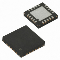
ATTINY24-20MU Atmel, ATTINY24-20MU Datasheet - Page 157

ATTINY24-20MU
Manufacturer Part Number
ATTINY24-20MU
Description
IC MCU AVR 2K FLASH 20MHZ 20-QFN
Manufacturer
Atmel
Series
AVR® ATtinyr
Specifications of ATTINY24-20MU
Core Processor
AVR
Core Size
8-Bit
Speed
20MHz
Connectivity
USI
Peripherals
Brown-out Detect/Reset, POR, PWM, Temp Sensor, WDT
Number Of I /o
12
Program Memory Size
2KB (1K x 16)
Program Memory Type
FLASH
Eeprom Size
128 x 8
Ram Size
128 x 8
Voltage - Supply (vcc/vdd)
2.7 V ~ 5.5 V
Data Converters
A/D 8x10b
Oscillator Type
Internal
Operating Temperature
-40°C ~ 85°C
Package / Case
20-MLF®, QFN
Processor Series
ATTINY2x
Core
AVR8
Data Bus Width
8 bit
Data Ram Size
128 B
Interface Type
USI
Maximum Clock Frequency
20 MHz
Number Of Programmable I/os
12
Number Of Timers
2
Operating Supply Voltage
2.7 V to 5.5 V
Maximum Operating Temperature
+ 85 C
Mounting Style
SMD/SMT
3rd Party Development Tools
EWAVR, EWAVR-BL
Development Tools By Supplier
ATAVRDRAGON, ATSTK500, ATSTK600, ATAVRISP2, ATAVRONEKIT
Minimum Operating Temperature
- 40 C
On-chip Adc
10 bit
For Use With
ATSTK600-DIP40 - STK600 SOCKET/ADAPTER 40-PDIP770-1007 - ISP 4PORT ATMEL AVR MCU SPI/JTAGATAVRISP2 - PROGRAMMER AVR IN SYSTEMATSTK505 - ADAPTER KIT FOR 14PIN AVR MCU
Lead Free Status / RoHS Status
Lead free / RoHS Compliant
Available stocks
Company
Part Number
Manufacturer
Quantity
Price
Part Number:
ATTINY24-20MU
Manufacturer:
AVNET
Quantity:
20 000
- Current page: 157 of 238
- Download datasheet (5Mb)
18.7
18.8
18.9
18.9.1
8006K–AVR–10/10
Preventing Flash Corruption
Programming Time for Flash when Using SPM
Register Description
SPMCSR – Store Program Memory Control and Status Register
If successful, the contents of the destination register are as described in section
ture Imprint Table” on page
During periods of low V
too low for the CPU and the Flash to operate properly. These issues are the same as for board
level systems using the Flash, and the same design solutions should be applied.
A Flash program corruption can be caused by two situations when the voltage is too low. First, a
regular write sequence to the Flash requires a minimum voltage to operate correctly. Secondly,
the CPU itself can execute instructions incorrectly, if the supply voltage for executing instructions
is too low.
Flash corruption can easily be avoided by following these design recommendations (one is
sufficient):
The calibrated RC Oscillator is used to time Flash accesses.
gramming time for Flash accesses from the CPU.
Table 18-1.
Note:
The Store Program Memory Control and Status Register contains the control bits needed to con-
trol the Program memory operations.
• Bits 7:6 – Res: Reserved Bits
These bits are reserved in the ATtiny24/44/84 and will always read as zero.
Bit
0x37 (0x57)
Read/Write
Initial Value
Flash write (Page Erase, Page Write, and
write Lock bits by SPM)
1. Keep the AVR RESET active (low) during periods of insufficient power supply voltage.
2. Keep the AVR core in Power-down sleep mode during periods of low V
This can be done by enabling the internal Brown-out Detector (BOD) if the operating
voltage matches the detection level. If not, an external low V
can be used. If a reset occurs while a write operation is in progress, the write operation
will be completed provided that the power supply voltage is sufficient.
vent the CPU from attempting to decode and execute instructions, effectively protecting
the SPMCSR Register and thus the Flash from unintentional writes.
1. The min and max programming times is per individual operation.
SPM Programming Time
Symbol
R
7
–
0
CC
, the Flash program can be corrupted because the supply voltage is
R
6
–
0
161.
RSIG
R
5
0
(1)
Min Programming Time
CTPB
R/W
4
0
3.7 ms
RFLB
R/W
3
0
PGWRT
Table 18-1
R/W
2
0
CC
ATtiny24/44/84
reset protection circuit
Max Programming Time
PGERS
R/W
1
0
shows the typical pro-
CC
. This will pre-
4.5 ms
SPMEN
R/W
“Device Signa-
0
0
SPMCSR
157
Related parts for ATTINY24-20MU
Image
Part Number
Description
Manufacturer
Datasheet
Request
R

Part Number:
Description:
Manufacturer:
Atmel Corporation
Datasheet:

Part Number:
Description:
Manufacturer:
Atmel Corporation
Datasheet:

Part Number:
Description:
IC MCU AVR 2K FLASH 20MHZ 14SOIC
Manufacturer:
Atmel
Datasheet:

Part Number:
Description:
MCU AVR 2K FLASH 15MHZ 20-QFN
Manufacturer:
Atmel
Datasheet:

Part Number:
Description:
IC MCU AVR 2K FLASH 20MHZ 14-DIP
Manufacturer:
Atmel
Datasheet:

Part Number:
Description:
MCU AVR 2KB FLASH 20MHZ 14SOIC
Manufacturer:
Atmel
Datasheet:

Part Number:
Description:
MCU AVR 2KB FLASH 20MHZ 20QFN
Manufacturer:
Atmel
Datasheet:

Part Number:
Description:
MCU AVR 2K FLASH 15MHZ 14-SOIC
Manufacturer:
Atmel
Datasheet:

Part Number:
Description:
DEV KIT FOR AVR/AVR32
Manufacturer:
Atmel
Datasheet:

Part Number:
Description:
INTERVAL AND WIPE/WASH WIPER CONTROL IC WITH DELAY
Manufacturer:
ATMEL Corporation
Datasheet:

Part Number:
Description:
Low-Voltage Voice-Switched IC for Hands-Free Operation
Manufacturer:
ATMEL Corporation
Datasheet:

Part Number:
Description:
MONOLITHIC INTEGRATED FEATUREPHONE CIRCUIT
Manufacturer:
ATMEL Corporation
Datasheet:


