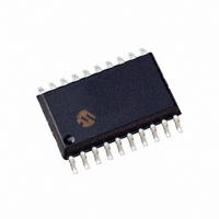
PIC24F16KA101-I/SO Microchip Technology, PIC24F16KA101-I/SO Datasheet - Page 106

PIC24F16KA101-I/SO
Manufacturer Part Number
PIC24F16KA101-I/SO
Description
IC PIC MCU FLASH 16K 20-SOIC
Manufacturer
Microchip Technology
Series
PIC® XLP™ 24Fr
Datasheets
1.MA240017.pdf
(254 pages)
2.PIC24F04KA201-ISS.pdf
(48 pages)
3.PIC24F16KA101-ISS.pdf
(18 pages)
Specifications of PIC24F16KA101-I/SO
Program Memory Type
FLASH
Program Memory Size
16KB (5.5K x 24)
Package / Case
20-SOIC (7.5mm Width)
Core Processor
PIC
Core Size
16-Bit
Speed
32MHz
Connectivity
I²C, IrDA, SPI, UART/USART
Peripherals
Brown-out Detect/Reset, POR, PWM, WDT
Number Of I /o
18
Eeprom Size
512 x 8
Ram Size
1.5K x 8
Voltage - Supply (vcc/vdd)
1.8 V ~ 3.6 V
Data Converters
A/D 9x10b
Oscillator Type
Internal
Operating Temperature
-40°C ~ 85°C
Processor Series
PIC24F
Core
PIC
Data Bus Width
16 bit
Data Ram Size
1.5 KB
Interface Type
I2C/IrDA/SPI/UART
Maximum Clock Frequency
32 MHz
Number Of Programmable I/os
18
Number Of Timers
3
Operating Supply Voltage
1.8 V to 3.6 V
Maximum Operating Temperature
+ 85 C
Mounting Style
SMD/SMT
3rd Party Development Tools
52713-733, 52714-737, 53276-922, EWDSPIC
Development Tools By Supplier
PG164130, DV164035, DV244005, DV164005, DM240001
Minimum Operating Temperature
- 40 C
On-chip Adc
9-ch x 10-bit
Lead Free Status / RoHS Status
Lead free / RoHS Compliant
For Use With
MA240017 - MODULE PLUG-IN PIC24F16KA102 PIM
Lead Free Status / Rohs Status
Lead free / RoHS Compliant
- Current page: 106 of 254
- Download datasheet (4Mb)
DSWDTOSC
postscaler
PIC24F16KA102 FAMILY
10.2.4.5
To enable the DSWDT in Deep Sleep mode, program
the Configuration bit, DSWDTEN (FDS<7>). The
device Watchdog Timer (WDT) need not be enabled for
the DSWDT to function. Entry into Deep Sleep mode
automatically resets the DSWDT.
The DSWDT clock source is selected by the
DSWDTPS<3:0> Configuration bits (FDS<3:0>). The
minimum time-out period that can be achieved is 2.1 ms
and the maximum is 25.7 days. For more details on the
FDS Configuration register and DSWDT configuration
options, refer to Section 26.0 “Special Features”.
10.2.4.6
Both the RTCC and the DSWDT may run from either
SOSC or the LPRC clock source. This allows both the
RTCC and DSWDT to run without requiring both the
LPRC and SOSC to be enabled together, reducing
power consumption.
Running the RTCC from LPRC will result in a loss of
accuracy in the RTCC of approximately 5 to 10%. If a
more accurate RTCC is required, it must be run from
the SOSC clock source. The RTCC clock source is
selected with the RTCOSC Configuration bit (FDS<5>).
Under certain circumstances, it is possible for the
DSWDT clock source to be off when entering Deep
Sleep mode. In this case, the clock source is turned on
automatically (if DSWDT is enabled), without the need
for software intervention. However, this can cause a
delay in the start of the DSWDT counters. In order to
avoid this delay when using SOSC as a clock source,
the application can activate SOSC prior to entering
Deep Sleep mode.
10.2.4.7
Upon entry into Deep Sleep mode, the status bit
DPSLP (RCON<10>), becomes set and must be
cleared by the software.
On power-up, the software should read this status bit to
determine if the Reset was due to an exit from Deep
Sleep mode and clear the bit if it is set. Of the four
possible combinations of DPSLP and POR bit states,
three cases can be considered:
• Both the DPSLP and POR bits are cleared. In this
• The DPSLP bit is clear, but the POR bit is set.
• Both the DPSLP and POR bits are set. This
DS39927B-page 104
case, the Reset was due to some event other
than a Deep Sleep mode exit.
This is a normal POR.
means that Deep Sleep mode was entered, the
device was powered down and Deep Sleep mode
was exited.
options
Deep Sleep WDT
Switching Clocks in Deep Sleep
Mode
Checking and Clearing the Status of
Deep Sleep
Configuration
are
programmed
bit
(FDS<4>).
by
The
Preliminary
the
10.2.4.8
V
ing from Deep Sleep functionally looks like a POR, the
technique described in Section 10.2.4.7 “Checking
and Clearing the Status of Deep Sleep” should be
used to distinguish between Deep Sleep and a true
POR event.
When a true POR occurs, the entire device, including
all Deep Sleep logic (Deep Sleep registers, RTCC,
DSWDT, etc.) is reset.
10.2.4.9
To review, these are the necessary steps involved in
invoking and exiting Deep Sleep mode:
1.
2.
3.
4.
5.
6.
7.
8.
9.
10. Device exits Deep Sleep when a wake-up event
11. The DSEN bit is automatically cleared.
12. Read and clear the DPSLP status bit in RCON,
13. Read the DSGPRx registers (optional).
14. Once all state related configurations are
15. Application resumes normal operation.
DD
Device exits Reset and begins to execute its
application code.
If DSWDT functionality is required, program the
appropriate Configuration bit.
Select the appropriate clock(s) for the DSWDT
and RTCC (optional).
Enable and configure the DSWDT (optional).
Enable and configure the RTCC (optional).
Write context data to the DSGPRx registers
(optional).
Enable the INT0 interrupt (optional).
Set the DSEN bit in the DSCON register.
Enter Deep Sleep by issuing a PWRSV
#SLEEP_MODE command.
occurs.
and the DSWAKE status bits.
complete, clear the RELEASE bit.
voltage is monitored to produce PORs. Since exit-
Power-on Resets (
Summary of Deep Sleep Sequence
© 2009 Microchip Technology Inc.
PORs
)
Related parts for PIC24F16KA101-I/SO
Image
Part Number
Description
Manufacturer
Datasheet
Request
R

Part Number:
Description:
Manufacturer:
Microchip Technology Inc.
Datasheet:

Part Number:
Description:
Manufacturer:
Microchip Technology Inc.
Datasheet:

Part Number:
Description:
Manufacturer:
Microchip Technology Inc.
Datasheet:

Part Number:
Description:
Manufacturer:
Microchip Technology Inc.
Datasheet:

Part Number:
Description:
Manufacturer:
Microchip Technology Inc.
Datasheet:

Part Number:
Description:
Manufacturer:
Microchip Technology Inc.
Datasheet:

Part Number:
Description:
Manufacturer:
Microchip Technology Inc.
Datasheet:

Part Number:
Description:
Manufacturer:
Microchip Technology Inc.
Datasheet:


