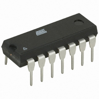
ATTINY84-20PU Atmel, ATTINY84-20PU Datasheet - Page 133

ATTINY84-20PU
Manufacturer Part Number
ATTINY84-20PU
Description
IC MCU AVR 8K FLASH 20MHZ 14-DIP
Manufacturer
Atmel
Series
AVR® ATtinyr
Specifications of ATTINY84-20PU
Core Processor
AVR
Core Size
8-Bit
Speed
20MHz
Connectivity
USI
Peripherals
Brown-out Detect/Reset, POR, PWM, Temp Sensor, WDT
Number Of I /o
12
Program Memory Size
8KB (4K x 16)
Program Memory Type
FLASH
Eeprom Size
512 x 8
Ram Size
512 x 8
Voltage - Supply (vcc/vdd)
2.7 V ~ 5.5 V
Data Converters
A/D 8x10b
Oscillator Type
Internal
Operating Temperature
-40°C ~ 85°C
Package / Case
14-DIP (0.300", 7.62mm)
Processor Series
ATTINY8x
Core
AVR8
Data Bus Width
8 bit
Data Ram Size
512 B
Interface Type
SPI
Maximum Clock Frequency
20 MHz
Number Of Programmable I/os
12
Number Of Timers
2
Operating Supply Voltage
2.7 V to 5.5 V
Maximum Operating Temperature
+ 85 C
Mounting Style
Through Hole
3rd Party Development Tools
EWAVR, EWAVR-BL
Development Tools By Supplier
ATAVRDRAGON, ATSTK500, ATSTK600, ATAVRISP2, ATAVRONEKIT
Minimum Operating Temperature
- 40 C
On-chip Adc
8-ch x 10-bit
Controller Family/series
AVR Tiny
No. Of I/o's
12
Eeprom Memory Size
512Byte
Ram Memory Size
512Byte
Cpu Speed
20MHz
No. Of Timers
2
Rohs Compliant
Yes
Package
14PDIP
Device Core
AVR
Family Name
ATtiny
Maximum Speed
20 MHz
For Use With
ATSTK600 - DEV KIT FOR AVR/AVR32770-1007 - ISP 4PORT ATMEL AVR MCU SPI/JTAGATAVRISP2 - PROGRAMMER AVR IN SYSTEM
Lead Free Status / RoHS Status
Lead free / RoHS Compliant
Available stocks
Company
Part Number
Manufacturer
Quantity
Price
Company:
Part Number:
ATTINY84-20PU
Manufacturer:
XILINX
Quantity:
25
- Current page: 133 of 238
- Download datasheet (5Mb)
16.3
8006K–AVR–10/10
Operation
Figure 16-1. Analog to Digital Converter Block Schematic
The ADC converts an analog input voltage to a 10-bit digital value through successive approxi-
mation. The minimum value represents GND and the maximum value represents the reference
voltage.The voltage reference for the ADC may be selected by writing to the REFS1:0 bits in
ADMUX. The VCC supply, the AREF pin or an internal 1.1V voltage reference may be selected
as the ADC voltage reference.
The analog input channel and differential gain are selected by writing to the MUX5:0 bits in
ADMUX. Any of the eight ADC input pins ADC7:0 can be selected as single ended inputs to the
ADC. For differential measurements all analog inputs next to each other can be selected as a
input pair. Every input is also possible to measure with ADC3. These pairs of differential inputs
are measured by ADC trough the differential gain amplifier.
ADC7
ADC6
ADC5
ADC4
ADC3
ADC2
ADC1
ADC0
AREF
V
CC
TEMPERATURE
REFERENCE
INTERNAL
8-BIT DATA BUS
AGND
ADC CTRL. & STATUS B
SENSOR
REGISTER (ADCSRB)
1.1V
ADC8
INPUT
INPUT
POS.
NEG.
ADTS2...ADTS0
MUX
MUX
ADC MULTIPLEXER
MUX DECODER
SELECT (ADMUX)
+
-
GAIN
AMPLIFIER
SINGLE ENDED / DIFFERENTIAL SELECTION
10-BIT DAC
ADC CTRL. & STATUS A
REGISTER (ADCSRA)
ADC CONVERSION
COMPLETE IRQ
PRESCALER
CONVERSION LOGIC
ATtiny24/44/84
INTERRUPT
TRIGGER
SELECT
FLAGS
SAMPLE & HOLD
COMPARATOR
15
+
-
ADC DATA REGISTER
(ADCH/ADCL)
ADC MULTIPLEXER
OUTPUT
0
133
Related parts for ATTINY84-20PU
Image
Part Number
Description
Manufacturer
Datasheet
Request
R

Part Number:
Description:
Manufacturer:
Atmel Corporation
Datasheet:

Part Number:
Description:
Manufacturer:
Atmel Corporation
Datasheet:

Part Number:
Description:
IC MCU AVR 8K FLASH 20MHZ 20-QFN
Manufacturer:
Atmel
Datasheet:

Part Number:
Description:
MCU AVR 8K ISP FLASH 2.7V 14SOIC
Manufacturer:
Atmel
Datasheet:

Part Number:
Description:
MCU AVR 8K FLASH 15MHZ 20-QFN
Manufacturer:
Atmel
Datasheet:

Part Number:
Description:
MCU AVR 8KB FLASH 10MHZ 14SOIC
Manufacturer:
Atmel
Datasheet:

Part Number:
Description:
MCU AVR 8KB FLASH 20MHZ 20QFN
Manufacturer:
Atmel
Datasheet:

Part Number:
Description:
DEV KIT FOR AVR/AVR32
Manufacturer:
Atmel
Datasheet:

Part Number:
Description:
INTERVAL AND WIPE/WASH WIPER CONTROL IC WITH DELAY
Manufacturer:
ATMEL Corporation
Datasheet:

Part Number:
Description:
Low-Voltage Voice-Switched IC for Hands-Free Operation
Manufacturer:
ATMEL Corporation
Datasheet:

Part Number:
Description:
MONOLITHIC INTEGRATED FEATUREPHONE CIRCUIT
Manufacturer:
ATMEL Corporation
Datasheet:

Part Number:
Description:
AM-FM Receiver IC U4255BM-M
Manufacturer:
ATMEL Corporation
Datasheet:

Part Number:
Description:
Monolithic Integrated Feature Phone Circuit
Manufacturer:
ATMEL Corporation
Datasheet:

Part Number:
Description:
Multistandard Video-IF and Quasi Parallel Sound Processing
Manufacturer:
ATMEL Corporation
Datasheet:


