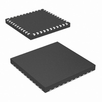
PIC18F47J13-I/ML Microchip Technology, PIC18F47J13-I/ML Datasheet - Page 541

PIC18F47J13-I/ML
Manufacturer Part Number
PIC18F47J13-I/ML
Description
IC PIC MCU 128KB FLASH 44QFN
Manufacturer
Microchip Technology
Series
PIC® XLP™ 18Fr
Datasheets
1.PIC18LF24J10-ISS.pdf
(32 pages)
2.PIC18F26J13-ISS.pdf
(496 pages)
3.PIC18F26J13-ISS.pdf
(558 pages)
4.PIC18F26J13-ISS.pdf
(12 pages)
Specifications of PIC18F47J13-I/ML
Core Size
8-Bit
Program Memory Size
128KB (64K x 16)
Core Processor
PIC
Speed
48MHz
Connectivity
I²C, LIN, SPI, UART/USART
Peripherals
Brown-out Detect/Reset, POR, PWM, WDT
Number Of I /o
34
Program Memory Type
FLASH
Ram Size
3.8K x 8
Voltage - Supply (vcc/vdd)
2.15 V ~ 3.6 V
Data Converters
A/D 13x10b/12b
Oscillator Type
Internal
Operating Temperature
-40°C ~ 85°C
Package / Case
*
Controller Family/series
PIC18
Cpu Speed
48MHz
Digital Ic Case Style
QFN
Supply Voltage Range
1.8V To 5.5V
Embedded Interface Type
I2C, SPI, USART
Rohs Compliant
Yes
Processor Series
PIC18F
Core
PIC
Data Bus Width
8 bit
Data Ram Size
4 KB
Interface Type
I2C, SPI, EUSART
Maximum Clock Frequency
48 MHz
Number Of Programmable I/os
25
Number Of Timers
8
Operating Supply Voltage
2 V to 3.6 V
Maximum Operating Temperature
+ 85 C
Mounting Style
SMD/SMT
3rd Party Development Tools
52715-96, 52716-328, 52717-734, 52712-325, EWPIC18
Development Tools By Supplier
DM164128, DM180021, DM183026-2, DV164131, MA180030, DM183022, DM183032, DV164136, MA180024
Minimum Operating Temperature
- 40 C
On-chip Adc
12 bit, 13 Channel
Lead Free Status / RoHS Status
Lead free / RoHS Compliant
For Use With
MA180030 - BOARD DEMO PIC18F47J13 FS USBMA180029 - BOARD DEMO PIC18F47J53 FS USB
Eeprom Size
-
Lead Free Status / Rohs Status
Details
- PIC18LF24J10-ISS PDF datasheet
- PIC18F26J13-ISS PDF datasheet #2
- PIC18F26J13-ISS PDF datasheet #3
- PIC18F26J13-ISS PDF datasheet #4
- Current page: 541 of 558
- Download datasheet (5Mb)
APPENDIX A:
Revision A (March 2010)
Original data sheet for PIC18F47J13 family devices.
TABLE B-1:
2010 Microchip Technology Inc.
Maximum Program Memory
Oscillator Options
SOSC Oscillator Options
T1CKI Clock Input
Timers
ECCP
CCP
SPI F
Option
Second I
ADC
Peripheral Module Disable
Bits
Band Gap Voltage Reference
Output
REPU/RDPU Pull-Up Enable
Bits
Comparators
Increased Output Drive
Strength
PWRT Period
OSC
Characteristic
2
/8 Master Clock
C™ Port
NOTABLE DIFFERENCES BETWEEN PIC18F47J13 AND PIC18F46J11 FAMILIES
REVISION HISTORY
13 Channel, 10/12-Bit Conversion modes
Three, each with four input pin selections.
Yes, enabled on pin, RA1, by setting the
PLL can be enabled at start-up with the
Low-power oscillator option for SOSC,
Moved to TRISE register (avoids read,
96 MHz PLL circuit is available via the
Default 4x PLL circuit is still available.
without enabling the Timer1 oscillator.
Yes, allowing further power reduction.
T1CKI can be used as a clock input
with Special Event Trigger option.
RA0 through RA5, RDx and REx.
Configuration bit setting, allowing
48 MHz operation from INTOSC.
VBGOE bit (WDTCON<4>).
Configuration bit option.
PIC18F47J13 Family
modify, write issues).
with run-time switch.
LF Devices – 46 ms
F Devices – 500
Yes, all packages.
128 Kbytes
Preliminary
Yes
8
3
7
s
PIC18F47J13 FAMILY
APPENDIX B:
Code for the devices in the PIC18F46J11 family can be
migrated to the PIC18F47J13 without many changes.
The differences between the two device families are
listed in Table B-1.
Pull-up bits configured in PORTE register
4x PLL circuit only. Maximum operating
Two, each with two input pin selections.
Requires firmware to set the PLLEN bit
Low-power oscillator option for SOSC,
only via the Configuration bit setting.
frequency from INTOSC is 32 MHz.
Yes, but only on 44-pin devices.
13 Channel, 10-bit only.
MIGRATION FROM
PIC18F46J11 TO
PIC18F47J13
LF Devices – 64 ms
18F46J11 Family
F Devices – 1 ms
at run time.
64 Kbytes
No
No
No
No
No
5
2
0
DS39974A-page 541
Related parts for PIC18F47J13-I/ML
Image
Part Number
Description
Manufacturer
Datasheet
Request
R

Part Number:
Description:
Manufacturer:
Microchip Technology Inc.
Datasheet:

Part Number:
Description:
Manufacturer:
Microchip Technology Inc.
Datasheet:

Part Number:
Description:
Manufacturer:
Microchip Technology Inc.
Datasheet:

Part Number:
Description:
Manufacturer:
Microchip Technology Inc.
Datasheet:

Part Number:
Description:
Manufacturer:
Microchip Technology Inc.
Datasheet:

Part Number:
Description:
Manufacturer:
Microchip Technology Inc.
Datasheet:

Part Number:
Description:
Manufacturer:
Microchip Technology Inc.
Datasheet:

Part Number:
Description:
Manufacturer:
Microchip Technology Inc.
Datasheet:


