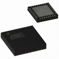
AT89C5130A-PUTUM Atmel, AT89C5130A-PUTUM Datasheet - Page 17

AT89C5130A-PUTUM
Manufacturer Part Number
AT89C5130A-PUTUM
Description
IC 8051 MCU FLASH 16K USB 32QFN
Manufacturer
Atmel
Series
AT89C513xr
Datasheet
1.AT89C5130A-PUTUM.pdf
(188 pages)
Specifications of AT89C5130A-PUTUM
Core Processor
C52X2
Core Size
8-Bit
Speed
48MHz
Connectivity
I²C, SPI, UART/USART, USB
Peripherals
LED, POR, PWM, WDT
Number Of I /o
18
Program Memory Size
16KB (16K x 8)
Program Memory Type
FLASH
Eeprom Size
4K x 8
Ram Size
1.25K x 8
Voltage - Supply (vcc/vdd)
2.7 V ~ 5.5 V
Oscillator Type
Internal
Operating Temperature
-40°C ~ 85°C
Package / Case
32-VQFN Exposed Pad, 32-HVQFN, 32-SQFN, 32-DHVQFN
Package
32QFN EP
Device Core
8051
Family Name
89C
Maximum Speed
48 MHz
Operating Supply Voltage
3.3|5 V
Data Bus Width
8 Bit
Number Of Programmable I/os
34
Interface Type
SPI/TWI/UART/USB
Number Of Timers
3
Processor Series
AT89x
Core
8051
Data Ram Size
1.25 KB
Maximum Clock Frequency
48 MHz
Maximum Operating Temperature
+ 85 C
Mounting Style
SMD/SMT
3rd Party Development Tools
PK51, CA51, A51, ULINK2
Development Tools By Supplier
AT89STK-05
Minimum Operating Temperature
- 40 C
Height
0.95 mm
Length
7 mm
Supply Voltage (max)
5.5 V
Supply Voltage (min)
2.7 V
Width
7 mm
For Use With
AT89OCD-01 - USB EMULATOR FOR AT8XC51 MCU
Lead Free Status / RoHS Status
Lead free / RoHS Compliant
Data Converters
-
Lead Free Status / Rohs Status
Details
Other names
AT89C5130A-PUTIM
AT89C5130A-PUTIM
AT89C5130A-PUTIM
Available stocks
Company
Part Number
Manufacturer
Quantity
Price
Company:
Part Number:
AT89C5130A-PUTUM
Manufacturer:
Atmel
Quantity:
5
5.4
4337K–USB–04/08
Registers
Table 5-2.
Bit Number
TWIX2
7
7
6
5
4
3
2
1
0
Oscillator Frequency
CKCON0 (S:8Fh)
Clock Control Register 0
32 MHz
40 MHz
Mnemonic Description
PCAX2
TWIX2
WDX2
WDX2
T2X2
T1X2
T0X2
SIX2
Bit
X2
6
TWI Clock
This control bit is validated when the CPU clock X2 is set. When X2 is low,
this bit has no effect.
Clear to select 6 clock periods per peripheral clock cycle.
Set to select 12 clock periods per peripheral clock cycle.
Watchdog Clock
This control bit is validated when the CPU clock X2 is set. When X2 is low,
this bit has no effect.
Clear to select 6 clock periods per peripheral clock cycle.
Set to select 12 clock periods per peripheral clock cycle.
Programmable Counter Array Clock
This control bit is validated when the CPU clock X2 is set. When X2 is low,
this bit has no effect.
Clear to select 6 clock periods per peripheral clock cycle.
Set to select 12 clock periods per peripheral clock cycle.
Enhanced UART Clock (Mode 0 and 2)
This control bit is validated when the CPU clock X2 is set. When X2 is low,
this bit has no effect.
Clear to select 6 clock periods per peripheral clock cycle.
Set to select 12 clock periods per peripheral clock cycle.
Timer2 Clock
This control bit is validated when the CPU clock X2 is set. When X2 is low,
this bit has no effect.
Clear to select 6 clock periods per peripheral clock cycle.
Set to select 12 clock periods per peripheral clock cycle.
Timer1 Clock
This control bit is validated when the CPU clock X2 is set. When X2 is low,
this bit has no effect.
Clear to select 6 clock periods per peripheral clock cycle.
Set to select 12 clock periods per peripheral clock cycle.
Timer0 Clock
This control bit is validated when the CPU clock X2 is set. When X2 is low,
this bit has no effect.
Clear to select 6 clock periods per peripheral clock cycle.
Set to select 12 clock periods per peripheral clock cycle.
System Clock Control bit
Clear to select 12 clock periods per machine cycle (STD mode, F
F
Set to select 6 clock periods per machine cycle (X2 mode, F
OSC
PCAX2
/
5
2).
R+1
12
3
SIX2
4
T2X2
3
AT89C5130A/31A-M
N+1
10
2
T1X2
2
T0X2
PLLDIV
CPU =
1
B9h
21h
CPU
F
PER =
= F
F
PER =
X2
OSC
0
).
17


