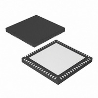
DSPIC33FJ128GP706A-I/MR Microchip Technology, DSPIC33FJ128GP706A-I/MR Datasheet - Page 23

DSPIC33FJ128GP706A-I/MR
Manufacturer Part Number
DSPIC33FJ128GP706A-I/MR
Description
IC DSPIC MCU/DSP 128K 64-QFN
Manufacturer
Microchip Technology
Series
dsPIC™ 33Fr
Datasheets
1.MCP3909T-ISS.pdf
(104 pages)
2.DSPIC33FJ12GP201-ISO.pdf
(90 pages)
3.DSPIC33FJ64GP206-IPT.pdf
(28 pages)
4.DSPIC33FJ64GP206A-IMR.pdf
(338 pages)
Specifications of DSPIC33FJ128GP706A-I/MR
Core Processor
dsPIC
Core Size
16-Bit
Speed
40 MIPs
Connectivity
CAN, I²C, IrDA, LIN, SPI, UART/USART
Peripherals
AC'97, Brown-out Detect/Reset, DMA, I²S, POR, PWM, WDT
Number Of I /o
53
Program Memory Size
128KB (128K x 8)
Program Memory Type
FLASH
Ram Size
16K x 8
Voltage - Supply (vcc/vdd)
3 V ~ 3.6 V
Data Converters
A/D 18x10b/12b
Oscillator Type
Internal
Operating Temperature
-40°C ~ 85°C
Package / Case
64-VFQFN, Exposed Pad
Product
DSCs
Processor Series
DSPIC33F
Core
dsPIC
3rd Party Development Tools
52713-733, 52714-737, 53276-922, EWDSPIC
Development Tools By Supplier
PG164130, DV164035, DV244005, DV164005, PG164120, DM240001, DV164033
Core Frequency
40MHz
Core Supply Voltage
3.3V
Embedded Interface Type
I2C, SPI, UART
No. Of I/o's
53
Flash Memory Size
128KB
Supply Voltage Range
3V To 3.6V
Rohs Compliant
No
Lead Free Status / RoHS Status
Lead free / RoHS Compliant
Eeprom Size
-
Lead Free Status / Rohs Status
Lead free / RoHS Compliant
58. Module: UART
59. Module: I/O
60. Module: SPI
© 2010 Microchip Technology Inc.
The UART module will not generate consecutive
break characters. Trying to perform a back-to-back
Break character transmission will cause the UART
module to transmit the dummy character used to
generate the first Break character instead of
transmitting the second Break character. Break
characters are generated correctly if they are
followed by non-Break character transmission.
Work around
None.
Affected Silicon Revisions
While the device is being programmed via the
PGECx/PGEDx pin pair, the device pin with SDO1
functionality may start toggling.
Work around
None.
Affected Silicon Revisions
Regardless of the Slave setting for the Frame
delay bit (FRMDLY = 0 or FRMDLY = 1), the Slave
always acts as if the sync pulse precedes the first
SPI data bit (FRMDLY = 0). The SPI will not
function as described if Slave FRMDLY = 1.
Work around
None.
Affected Silicon Revisions
A2
A2
A2
X
X
X
A3
A3
A3
X
X
X
A4
A4
A4
X
X
X
61. Module: ADC
If the ADC module is in an enabled state when the
device enters Sleep mode as a result of executing
a PWRSAV #0 instruction, the device power-down
current (I
in the device data sheet. This may happen even if
the ADC module is disabled by clearing the ADON
bit prior to entering Sleep mode.
Work around
In order to remain within the I
listed in the device data sheet, the user software
must completely disable the ADC module by
setting the ADC Module Disable bit in the
corresponding Peripheral Module Disable register
(PMDx), prior to executing a PWRSAV
instruction.
Affected Silicon Revisions
A2
X
A3
X
PD
) may exceed the specifications listed
A4
X
DS80446D-page 23
PD
specifications
#0


