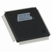
AT91M40800-33AU Atmel, AT91M40800-33AU Datasheet - Page 8

AT91M40800-33AU
Manufacturer Part Number
AT91M40800-33AU
Description
IC ARM7 MCU 100 LQFP
Manufacturer
Atmel
Series
AT91SAMr
Specifications of AT91M40800-33AU
Core Processor
ARM7
Core Size
16/32-Bit
Speed
33MHz
Connectivity
EBI/EMI, UART/USART
Peripherals
POR, WDT
Number Of I /o
32
Program Memory Type
ROMless
Ram Size
8K x 8
Voltage - Supply (vcc/vdd)
1.8 V ~ 3.6 V
Oscillator Type
External
Operating Temperature
-40°C ~ 85°C
Package / Case
100-LQFP
Package
100TQFP
Device Core
ARM7TDMI
Family Name
91M
Maximum Speed
33 MHz
Operating Supply Voltage
2.5|3.3 V
Data Bus Width
32 Bit
Number Of Programmable I/os
32
Interface Type
EBI/USART
Number Of Timers
3
Processor Series
AT91Mx
Core
ARM7TDMI
Data Ram Size
8 KB
Maximum Clock Frequency
33 MHz
Maximum Operating Temperature
+ 85 C
Mounting Style
SMD/SMT
3rd Party Development Tools
JTRACE-ARM-2M, MDK-ARM, RL-ARM, ULINK2
Minimum Operating Temperature
- 40 C
Eeprom Memory
0 Bytes
Input Output
32
Interface
EBI/EMI, UART/USART
Ios
32
Memory Type
ROMless
Number Of Bits
32
Package Type
100-pin LQFP
Programmable Memory
0 Bytes
Timers
3-16-bit
Voltage, Range
1.8-3.6 V
Cpu Family
91M
Device Core Size
32b
Frequency (max)
33MHz
Program Memory Size
Not Required
Total Internal Ram Size
8KB
# I/os (max)
32
Number Of Timers - General Purpose
3
Operating Supply Voltage (typ)
2.5/3.3V
Operating Supply Voltage (max)
3.6V
Operating Supply Voltage (min)
1.8V
Instruction Set Architecture
RISC
Operating Temp Range
-40C to 85C
Operating Temperature Classification
Industrial
Mounting
Surface Mount
Pin Count
100
Lead Free Status / RoHS Status
Lead free / RoHS Compliant
Eeprom Size
-
Program Memory Size
-
Data Converters
-
Lead Free Status / Rohs Status
Lead free / RoHS Compliant
Available stocks
Company
Part Number
Manufacturer
Quantity
Price
Company:
Part Number:
AT91M40800-33AU
Manufacturer:
ATMEL
Quantity:
1 000
Company:
Part Number:
AT91M40800-33AU
Manufacturer:
ATMEL
Quantity:
346
Part Number:
AT91M40800-33AU
Manufacturer:
ATMEL/爱特梅尔
Quantity:
20 000
7.5.2
7.6
7.6.1
7.6.2
8
Memory Controller
AT91M40800
JTAG/ICE Debug
Internal Memories
Boot Mode Select
To enter Tri-state mode, the pin NTRI must be held low during the last 10 clock cycles before the
rising edge of NRST. For normal operation the pin NTRI must be held high during reset by a
resistor of up to 400K Ohm.
NTRI is multiplexed with I/O line P21 and USART1 serial data transmit line TXD1.
Standard RS232 drivers generally contain internal 400K Ohm pull-up resistors. If TXD1 is con-
nected to a device not including this pull-up, the user must make sure that a high level is tied on
NTRI while NRST is asserted.
ARM Standard Embedded In-circuit Emulation is supported via the JTAG/ICE port. The pins
TDI, TDO, TCK and TMS are dedicated to this debug function and can be connected to a host
computer via the external ICE interface.
In ICE Debug mode, the ARM7TDMI core responds with a non-JTAG chip ID that identifies the
microcontroller. This is not fully IEEE
The ARM7TDMI processor address space is 4G bytes. The memory controller decodes the
internal 32-bit address bus and defines three address spaces:
In any of these address spaces, the ARM7TDMI operates in Little-Endian mode only.
The AT91M40800 microcontroller integrates 8K bytes of internal SRAM. All internal memories
are 32 bits wide and single-clock cycle accessible. Byte (8-bit), half-word (16-bit) or word (32-bit)
accesses are supported and are executed within one cycle. Fetching Thumb or ARM instruc-
tions is supported and internal memory can store twice as many Thumb instructions as ARM
ones.
The SRAM is mapped at address 0x0 (after the remap command), allowing ARM7TDMI excep-
tion vectors between 0x0 and 0x20 to be modified by the software. The rest of the bank can be
used for stack allocation (to speed up context saving and restoring) or as data and program stor-
age for critical algorithms.
The ARM reset vector is at address 0x0. After the NRST line is released, the ARM7TDMI exe-
cutes the instruction stored at this address. This means that this address must be mapped in
nonvolatile memory after the reset.
The input level on the BMS pin during the last 10 clock cycles before the rising edge of the
NRST selects the type of boot memory (see
• Internal memories in the four lowest megabytes
• Middle space reserved for the external devices (memory or peripherals) controlled by the EBI
• Internal peripherals in the four highest megabytes
®
1149.1 compliant.
Table
7-1).
1348FS–ATARM–13-Apr-06


