AT89C5132-ROTUL Atmel, AT89C5132-ROTUL Datasheet
AT89C5132-ROTUL
Specifications of AT89C5132-ROTUL
Available stocks


Related parts for AT89C5132-ROTUL


AT89C5132-ROTUL Summary of contents
Page 1
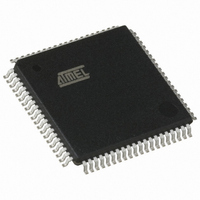
... TQFP80, PLCC84 (Development Board Only) – Dice Description The AT89C5132 is a mass storage device controlling data exchange between various Flash modules, HDD and CD-ROM. The AT89C5132 includes 64K Bytes of Flash memory and allows In-System Program- ming through an embedded 4K Bytes of Boot Flash Memory. ...
Page 2
... Block Diagram Figure 1. AT89C5132 Block Diagram INT0 INT1 Interrupt Handler Unit RAM 2304 Bytes C51 (X2 CORE) Clock and PLL Unit FILT X1 X2 RST DOUT Notes: 1. Alternate function of Port 3 2. Alternate function of Port 4 3. Alternate function of Port 1 AT89C5132 4 AV UVSS AVSS AREF ...
Page 3
... Pin Description 4173CS–USB–07/04 Figure 2. AT89C5132 80-pin TQFP Package ALE 1 ISP 2 P1.0/KIN0 3 P1.1/KIN1 4 P1.2/KIN2 5 P1.3/KIN3 6 P1.4 7 P1.5 8 P1.6/SCL 9 P1.7/SDA 10 VDD 11 PVDD 12 FILT 13 PVSS 14 VSS TST 18 UVDD 19 UVSS 20 AT89C5132 TQFP80 P4.5 P4.4 P2.2/A10 P2.3/A11 P2.4/A12 P2.5/A13 P2.6/A14 P2.7/A15 VSS VDD MCLK ...
Page 4
... AT89C5132 6 Figure 3. AT89C5132 84-pin PLCC ALE 12 ISP 13 P1.0/KIN0 14 P1.1/KIN1 15 P1.2/KIN2 16 P1.3/KIN3 17 P1.4 18 P1.5 19 P1.6/SCL 20 P1.7/SDA 21 VDD 22 PAVDD 23 FILT 24 PAVSS 25 VSS TST 30 UVDD 31 UVSS 32 Note: 1. For development board only. ( PLCC84 P4.5 P4.4 P2.2/A10 P2.3/A11 P2.4/A12 P2.5/A13 P2.6/A14 P2.7/A15 VSS VDD MCLK MDAT ...
Page 5
... Signals 4173CS–USB–07/04 All the AT89C5132 signals are detailed by functionality in Table 1 to Table 15. Table 1. Ports Signal Description Signal Name Type Description Port 8-bit open-drain bidirectional I/O port. Port 0 pins that have 1s P0.7:0 I/O written to them float and can be used as high impedance inputs. To ...
Page 6
... AT89C5132 8 Table 3. Timer 0 and Timer 1 Signal Description Signal Name Type Description Timer 0 Gate Input INT0 serves as external run control for timer 0, when selected by GATE0 bit in TCON register. INT0 I External Interrupt 0 INT0 input sets IE0 in the TCON register. If bit IT0 in this register is set, bit IE0 is set by a falling edge on INT0# ...
Page 7
... When TWI controller is in master mode, SCL outputs the serial clock to SCL I/O the slave peripherals. When TWI controller is in slave mode, SCL receives clock from the master controller. TWI Serial Data SDA I/O SDA is the bidirectional Two Wire data line. AT89C5132 Alternate Function - - ...
Page 8
... AT89C5132 10 Table 11. A/D Converter Signal Description Signal Name Type Description AIN1:0 I A/D Converter Analog Inputs AREFP I Analog Positive Voltage Reference Input Analog Negative Voltage Reference Input AREFN I This pin is internally connected to AVSS. Table 12. Keypad Interface Signal Description Signal Name Type Description ...
Page 9
... Connect this pin to +3V supply voltage. PLL Circuit Ground PVSS GND Connect this pin to ground. USB Supply Voltage UVDD PWR Connect this pin to +3V supply voltage. USB Ground UVSS GND Connect this pin to ground. AT89C5132 Alternate Function is applied, whether or not the Alternate Function ...
Page 10
... Internal Pin Structure AT89C5132 12 Table 16. Detailed Internal Pin Structure Circuit VDD Watchdog Output 2 osc periods Latch Output Notes: 1. For information on resistors value, input/output levels, and drive capability, refer to the Section “DC Characteristics”, page 183. 2. When the Two Wire controller is enabled, P allowing pseudo open-drain structure ...
Page 11
... Thanks to the internal charge pump, the high voltage needed for pro- gramming or erasing Flash cells is generated on-chip using the standard V Thus, the AT89C5132 can be programmed using only one voltage and allows in applica- tion software programming commonly known as IAP. Hardware programming mode is also available using specific programming tools ...
Page 12
... Universal Serial Bus Interface MultiMedia Card Interface IDE/ATAPI Interface AT89C5132 16 The AT8xC5132 peripherals are briefly described in the following sections. For further details on how to interface (hardware and software) to these peripherals, please refer to the AT8xC5132 complete datasheet. The AT8xC5132 internal clocks are extracted from an on-chip PLL fed by an on-chip oscillator ...
Page 13
... Interface Two-wire Controller A/D Controller 4173CS–USB–07/04 The AT89C5132 implements a serial port with its own baud rate generator providing one single synchronous communication mode and three full-duplex Universal Asynchronous Receiver Transmitter (UART) communication modes provided for the following purposes: • ...
Page 14
... OH2 MDAT, MCLK, SCLK, DCLK, DSEL, DOUT, D+, D-) Logical 0 Input Current (P1, P2, P3 and P5) AT89C5132 18 NOTE: Stressing the device beyond the “Absolute Maxi- mum Ratings” may cause permanent damage. -0.3 to +4.0V These are stress ratings only. Operation beyond the “operating conditions” is not recommended and extended exposure beyond the “ ...
Page 15
... See Table 154 for typical consumption in player mode. Figure 1. I Test Condition, Active Mode DD VDD RST (NC) X2 Clock Signal X1 VSS PVSS UVSS AVSS VSS All other pins are unconnected AT89C5132 (1) Max Units µA 10 0.45< V µA -650 Vin = 2.0 V 200 kΩ 25° ...
Page 16
... AT89C5132 20 Figure 2. I Test Condition, Idle Mode DL RST VSS (NC) X2 Clock Signal X1 VSS PVSS UVSS AVSS VSS All other pins are unconnected Figure 3. I Test Condition, Power-Down Mode PD RST VSS (NC VSS PVSS UVSS AVSS VSS All other pins are unconnected VDD ...
Page 17
... Table 3. Oscillator and Crystal Characteristics V = 2 -40° to +85° Symbol Parameter V C Internal Capacitance ( Internal Capacitance ( Equivalent Load Capacitance ( Drive Level F Crystal Frequency RS Crystal Series Resistance CS Crystal Shunt Capacitance AT89C5132 Min Typ Max Units 2.7 3.3 V µA 600 µ 2 kΩ ...
Page 18
... Phase Lock Loop Schematic Parameters USB Connection Schematic Parameters In-system Programming Schematic Parameters AT89C5132 22 Figure 5. PLL Filter Connection FILT Table 4. PLL Filter Characteristics V = 2 -40° to +85° Symbol Parameter R Filter Resistor C1 Filter Capacitance 1 C2 Filter Capacitance 2 Figure 6. USB Connection VBUS ...
Page 19
... AVDV T Address Valid to RD Low AVRL T RD Low to Valid Data RLDV T RD Low to Address Float RLAZ T Data Hold After RD High RHDX Instruction Float After RD T RHDZ High AT89C5132 Conditions Variable Clock Variable Clock Standard Mode X2 Mode Min Max Min 50 50 2·T ...
Page 20
... Waveforms AT89C5132 24 Table 3. External 8-bit Bus Cycle – Data Write AC Timings V = 2.7 to 3.3V -40° to +85° Symbol Parameter T Clock Period CLCL T ALE Pulse Width 2·T LHLL T Address Valid to ALE Low T AVLL Address hold after ALE T T LLAX Low T ALE Low to WR Low 3· ...
Page 21
... T T AVLL LLAX P0 A7:0 P2 Table 4. External IDE 16-bit Bus Cycles Timing Symbol Definitions Signals A Address D Data In L ALE Q Data Out Test conditions: capacitive load on all pins = 50 pF. AT89C5132 LLWL WLWH WHLH T T QVWH WHQX D7:0 Data Out A15:8 Conditions High Low ...
Page 22
... AT89C5132 26 Table 5. External IDE 16-bit Bus Cycle – Data Read AC Timings V = 2.7 to 3.3V -40° to +85° Symbol Parameter T Clock Period CLCL T ALE Pulse Width LHLL T Address Valid to ALE Low AVLL T Address hold after ALE Low LLAX T ALE Low to RD Low LLRL ...
Page 23
... LHLL WR T AVWL T T AVLL LLAX P0 A7:0 P2 A15:8 Note: D15:8 is the content of DAT16H SFR. Table 7. SPI Interface Timing Symbol Definitions Signals C Clock I Data In O Data Out AT89C5132 T T LLRL RLRH RHLH T RLDV T RHDZ T RHDX D7:0 Data In AVDV D15:81 Data LLWL WLWH ...
Page 24
... Timings AT89C5132 28 Table 8. SPI Interface Master AC Timing V = 2.7 to 3.3V -40° to +85° Symbol Parameter T Clock Period CHCH T Clock High Time CHCX T Clock Low Time CLCX Low to Clock edge SLCH SLCL Input Data Valid to Clock Edge IVCL IVCH Input Data Hold after Clock Edge ...
Page 25
... IVCL CLIX MSB IN BIT 6 T CHCH T T CHCX CLCX T T IVCH CHIX T T IVCL CLIX MSB IN BIT 6 T CLOV T CHOV MSB OUT BIT 6 AT89C5132 T CLSH T T SHSL CHSH T CLCH T CHCL T CLOX T T SHOX CHOX 1 LSB IN T CLCH T CHCL LSB IN T CLOX ...
Page 26
... SS handled by software using general purpose port pin. Figure 8. SPI Master Waveforms (SSCPHA = 1) SS1 (output) SCK (SSCPOL = 0) (output) SCK (SSCPOL = 1) (output) SI (input) SO (output) Note handled by software using general purpose port pin. AT89C5132 30 T SLCH T T SLCL CHCH T T CHCX CLCX T T SLOV T ...
Page 27
... T = one oscillator clock period. CLCL OSC Figure 9. Two Wire Waveforms ;STA T DAT high Tsu;DAT1 low hd hd; AT89C5132 INPUT Min Max 14·T CLCL 16·T CLCL 14·T CLCL 1 µs 0.3 µs 250 ns 250 ns 250 14·T CLCL 14·T CLCL 14·T CLCL 1 µs 0.3 µs ...
Page 28
... MMC Interface Definition of Symbols Timings Waveforms AT89C5132 32 Table 9. MMC Interface Timing Symbol Definitions Signals C Clock D Data In O Data Out Table 10. MMC Interface AC Timings = -40 to +85°C, CL ≤ 100pF (10 cards 2 Symbol Parameter T Clock Period CHCH T Clock High Time CHCX T Clock Low Time ...
Page 29
... T Clock Rise Time CLCH T Clock Fall Time CHCL T Clock Low to Select Valid CLSV T Clock Low to Data Valid CLOV Note: 32-bit format with kHz. Figure 11. Audio Interface Waveforms DCLK DSEL Right T CLOV DDAT AT89C5132 Conditions Min Max (1) 325 CHCH T T CHCX CLCX ...
Page 30
... Analog to Digital Converter Definition of Symbols Characteristics Waveforms Figure 12. Analog-to-Digital Converter Internal Waveforms CLK ADEN Bit T EHSH ADSST Bit AT89C5132 34 Table 13. Analog to Digital Converter Timing Symbol Definitions Signals C Clock E Enable (ADEN bit) Start Conversion S (ADSST bit) Table 2. Analog to Digital Converter AC Characteristics V = 2 -40 to +85° ...
Page 31
... Input ISP Valid to RST Edge SVRL T Input ISP Hold after RST Edge RLSX T FLASH Internal Busy (Programming) Time BHBL N Number of Flash Write Cycles FCY T Flash Data Retention Time FDR AT89C5132 Offset Gain Error Error OSe Ge Example of an Actual Transfer Curve AVIN (LSBideal) Conditions Min ...
Page 32
... Waveforms External Clock Drive and Logic Level References Definition of Symbols Timings Waveforms AT89C5132 36 Figure 14. Flash Memory – ISP Waveforms RST (1) ISP Note: 1. ISP must be driven through a pull-down resistor (see Section “In-system Program- ming”, page 22). Figure 15. Flash Memory – Internal Busy Waveforms FBUSY bit Table 16 ...
Page 33
... V 4173CS–USB–07/04 INPUTS -0.5V for a logic 1 and 0.45V for a logic 0. DD min for a logic 1 and 0.1V LOAD Timing Reference Points V - 0.1V LOAD = ±20 mA. /V level occurs with AT89C5132 OUTPUTS V min IH V max IL max for a logic 0. 0. ...
Page 34
... Ordering Information (1) Possible Order Entries Memory Size Part Number (Bytes) AT89C5132-ROTIL 64K Flash Note: 1. PLCC84 package only available for development board. AT89C5132 38 Max Temperature Supply Frequency Voltage Range (MHz) 3V Industrial 40 Product Package Packing Marking TQFP80 Tray 895132-IL 4173CS–USB–07/04 ...
Page 35
... Package Information TQFP80 4173CS–USB–07/04 AT89C5132 39 ...
Page 36
... PLCC84 AT89C5132 40 4173CS–USB–07/04 ...
Page 37
... Datasheet Change Log for AT89C5132 Changes from 4173A- 08/02 to 4173B-03/04 Changes from 4173B- 03/04 - 4173C - 07/04 4173CS–USB–07/04 1. Supression of ROM product version. 2. Supression of TQFP64 package. 1. Add USB connection schematic in USB section. 2. Add USB termination characteristics in DC Characteristics section. 3. Page access mode clarification in Data Memory section. ...
Page 38
... No licenses to patents or other intellectual property of Atmel are granted by the Company in connection with the sale of Atmel products, expressly or by implication. Atmel’s products are not authorized for use as critical components in life support devices or systems. ...